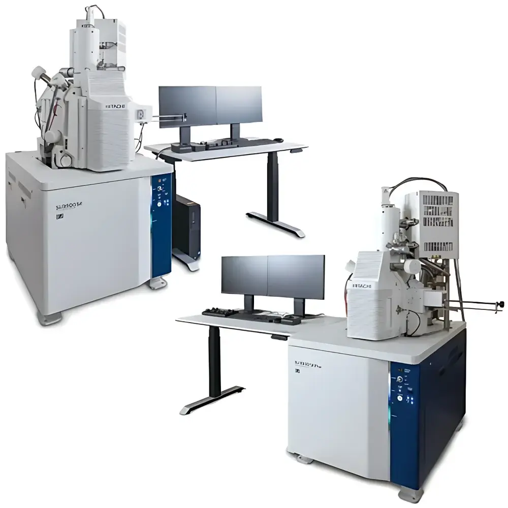
Hitachi SU3900/SU3800 SE Series High-Resolution Thermal Field-Emission Scanning Electron Microscope
| Brand | Hitachi |
|---|---|
| Origin | Japan |
| Manufacturer Type | Original Equipment Manufacturer (OEM) |
| Product Origin | Imported |
| Model | SU3900/SU3800 SE Series |
| Instrument Type | Floor-Standing Conventional SEM |
| Electron Source | Thermal Field-Emission Gun |
| Secondary Electron Resolution | 0.9 nm @ 30 kV, 2.5 nm @ 1 kV, 1.6 nm @ 1 kV (Deceleration Mode) |
| Magnification Range | ×5 to ×600,000 (Film Equivalent) |
| Accelerating Voltage | 0.5 kV to 30 kV |
Overview
The Hitachi SU3900/SU3800 SE Series represents a class of high-performance thermal field-emission scanning electron microscopes (FE-SEM) engineered for industrial and advanced materials research applications requiring both high spatial resolution and exceptional operational flexibility. Unlike conventional SEM platforms constrained by sample size, weight, or conductivity limitations, this series integrates a robust mechanical architecture with an optimized electron optical column and a large-volume specimen chamber—enabling direct observation of bulk engineering components without sectioning, mounting, or conductive coating. Its thermal field-emission electron source delivers stable, high-brightness beams across the full accelerating voltage range (0.5–30 kV), supporting high-resolution secondary electron (SE) imaging at both high and low kV—critical for surface-sensitive analysis of insulators, nanoscale features, and topographically complex specimens. The system is designed for compliance with ISO/IEC 17025 laboratory accreditation requirements and supports GLP/GMP-aligned workflows through audit-trail-capable software logging.
Key Features
- Thermal field-emission electron gun with extended lifetime and beam stability under variable vacuum conditions (including low-vacuum mode for non-conductive samples)
- Large specimen chamber accommodating samples up to Ø300 mm in diameter and 45 mm in height—compatible with industrial components such as automotive castings, aerospace turbine blades, and full 300-mm wafers
- Dual-mode SE detection: In-lens detector for high-resolution surface imaging and Everhart-Thornley detector for wide-field contrast; optional Ultra-Violet Detector (UVD) for complementary signal acquisition (e.g., cathodoluminescence, low-energy SE)
- Standard high-sensitivity backscattered electron (BSE) detector with compositional and topographic contrast separation, enhanced by deceleration optics for improved surface sensitivity at 1 kV
- Automated optical alignment routines—including stigmator correction, focus optimization, and brightness/contrast balancing—reducing operator dependency and improving inter-user reproducibility
- Modular workflow automation via optional EM Flow Creator software, enabling drag-and-drop creation of multi-step acquisition protocols (e.g., area-based low-/mid-/high-mag imaging sequences with stage positioning, focus adjustment, and detector switching)
Sample Compatibility & Compliance
The SU3900/SU3800 SE Series eliminates common SEM preparation bottlenecks. Non-conductive samples—including ceramics, polymers, biological composites, and uncoated geological specimens—can be imaged directly in low-vacuum mode without carbon/metal sputter coating. Its rigid stage design and motorized tilt/rotation capabilities support multi-angle imaging of oversized parts, satisfying ASTM E1558 (Standard Guide for SEM Use in Fractography) and ISO 22453 (Microbeam analysis — SEM — Measurement of resolution). All models comply with IEC 61000-6-3 (EMC emission standards) and meet CE marking requirements for safe operation in regulated laboratory environments. Data integrity is maintained per FDA 21 CFR Part 11 when used with validated software configurations and electronic signature modules.
Software & Data Management
Acquisition and analysis are managed through Hitachi’s proprietary SEM Control Software, which supports DICOM-compatible image export, TIFF/PNG metadata embedding (including kV, WD, magnification, detector type, and timestamp), and batch annotation. Raw image data retain full dynamic range (16-bit depth) and are stored in vendor-neutral formats compatible with third-party quantification tools (e.g., ImageJ/Fiji, MATLAB, Thermo Scientific Avizo). Audit trails record all user actions—including parameter changes, stage movements, and detector selections—with time stamps and operator IDs. Optional EM Flow Creator enables protocol-driven acquisition with version-controlled script libraries, facilitating SOP implementation across multi-site manufacturing QA labs.
Applications
- Metallurgy & Failure Analysis: High-tilt SE imaging of fracture surfaces (e.g., ductile voids in steel wire cross-sections); BSE phase mapping of multiphase alloys (e.g., high-entropy carbide films)
- Electronics & Semiconductors: Cross-sectional inspection of MLCCs (multilayer ceramic capacitors) revealing Ni electrode continuity and dielectric grain structure; surface topology analysis of lithographically patterned wafers
- Energy Materials: Distribution analysis of LiCoO₂ cathode particles and binder matrix interfaces; surface coverage quantification of graphite anode coatings
- Advanced Ceramics & Nanomaterials: Morphological characterization of ZnO nanoparticles (~50 nm) and agglomeration behavior in composite matrices
- Automotive & Aerospace: In situ observation of thermal barrier coating delamination, fatigue crack initiation sites, and additive-manufactured part porosity
FAQ
Does the SU3900/SU3800 SE Series require conductive coating for non-metallic samples?
No—low-vacuum imaging mode (down to 10 Pa) suppresses charging effects on insulators, enabling direct observation of uncoated polymers, ceramics, and biological specimens.
What is the minimum working distance required to achieve the specified 0.9 nm resolution?
The 0.9 nm specification is validated at a working distance of 4 mm and 30 kV using the in-lens SE detector under ultra-high vacuum conditions.
Can the system be integrated into automated factory-floor inspection workflows?
Yes—via EM Flow Creator and Ethernet-based remote control APIs, the microscope supports integration with MES systems and programmable logic controllers (PLCs) for inline QA/QC deployment.
Is the BSE detector capable of qualitative elemental differentiation?
While not a quantitative EDS system, the standard BSE detector provides atomic number (Z)-dependent contrast suitable for distinguishing phases with ΔZ ≥ 5 (e.g., Al vs. Si, Fe vs. Cr) in polished sections.
How does the deceleration mode improve surface sensitivity at 1 kV?
Beam deceleration reduces landing energy while maintaining high gun extraction voltage, yielding improved signal-to-noise ratio and reduced penetration depth—ideal for analyzing native oxide layers or thin-film interfaces.


