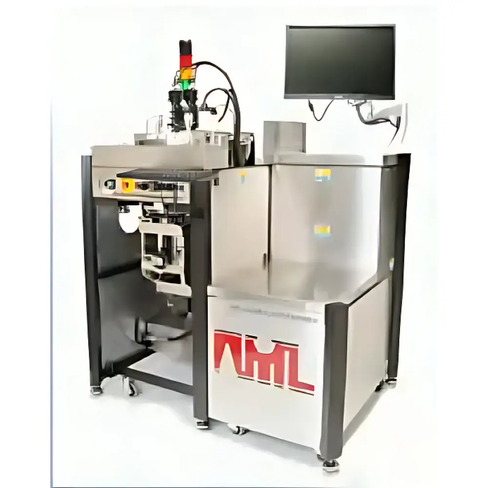
AML AWB-04 In-Situ Wafer Bonding System
| Brand | AML |
|---|---|
| Origin | USA |
| Manufacturer Type | Authorized Distributor |
| Origin Category | Imported |
| Model | AWB-04 |
| Pricing | Upon Request |
Overview
The AML AWB-04 In-Situ Wafer Bonding System is a precision-engineered platform designed for high-accuracy, vacuum-compatible wafer bonding in research and pilot-line semiconductor fabrication environments. Developed by Applied Microengineering Ltd. (AML), a UK-based specialist founded in 1992 and headquartered at the Harwell Science and Innovation Campus, the AWB-04 implements a true in-situ workflow—integrating real-time alignment, surface activation (including plasma and formic acid vapor treatment), and thermocompression or anodic bonding within a single vacuum chamber. This eliminates inter-process contamination, thermal drift, and mechanical repositioning errors common in multi-chamber systems. The system supports bonding of silicon, fused silica, sapphire, glass, and metalized wafers (e.g., Cu–Cu) across diameters from 50 mm (2″) to 300 mm, with stack height up to 6.5 mm. Its architecture complies with cleanroom Class 100 requirements and features base pressure down to 1 × 10⁻⁶ mbar, achieved in under 5 minutes—enabling high-fidelity vacuum bonding essential for MEMS encapsulation, TSV-based 3D integration, and wafer-level packaging (WLP).
Key Features
- In-situ alignment, activation, and bonding in one vacuum chamber—eliminating transfer-induced misalignment and interface contamination
- Independent top/bottom chuck heating (up to >300 °C) with real-time temperature profiling; supports getter material integration and formic acid vapor oxide reduction for Cu–Cu bonding
- Automated sub-micron alignment (≤1 µm overlay accuracy) using backside mark imaging and motorized theta-Z compensation
- Programmable force control (up to 25 kN) with closed-loop load monitoring and dynamic pressure mapping during bond cycle
- Integrated plasma activation module for native oxide removal and surface functionalization prior to bonding
- Vacuum-compatible temporary bonding solution—adhesive-free, with bond time <5 min and debond time <10 min—optimized for 3D-IC redistribution layer (RDL) and thin-wafer handling
- Modular load port options: FOUP, SMIF, or open cassette (2–3 ports), supporting automated wafer transfer in fab-integrated workflows
Sample Compatibility & Compliance
The AWB-04 accommodates standard semiconductor substrates including Si, SiO₂, SiNₓ, glass (e.g., Borofloat®, Pyrex®), sapphire, and metal-coated wafers (Al, Ti, Cu, Au). It supports both permanent (thermocompression, anodic, eutectic) and temporary (vacuum adhesion) bonding schemes. Process repeatability meets ISO 9001-certified manufacturing protocols. All bonding recipes are traceable and auditable per FDA 21 CFR Part 11 requirements when paired with AML’s certified software suite. The system is compatible with SEMI MS5-0813 (“Micro Chevron Testing”) for bond strength validation and supports GLP/GMP documentation workflows for qualification-limited production environments.
Software & Data Management
Control and analysis are managed via AML’s BondStudio™ software—a Windows-based, role-secured application with full recipe management, real-time parameter logging (temperature, pressure, force, time), and automated report generation. Data export conforms to ASTM E1447 and SEMI E137 standards. Integrated image acquisition enables automatic fiducial recognition and alignment offset correction. For post-bond evaluation, the system interfaces seamlessly with IRIS infrared inspection and Maszara bond strength analyzers—enabling correlation of alignment accuracy, bond integrity, and mechanical strength across full-wafer maps. Audit trails include user ID, timestamp, versioned recipe, and raw sensor logs—fully compliant with electronic record retention policies.
Applications
- MEMS vacuum packaging and cavity sealing (e.g., gyroscopes, accelerometers)
- Wafer-level packaging (WLP) for RF, optical, and power devices
- 3D IC integration via TSVs, microbumps, and direct Cu–Cu bonding
- Advanced substrate bonding for heterogeneous integration (Si-on-glass, III–V on Si)
- Temporary bonding/debonding for thin-wafer processing and grinding
- Nanoimprint lithography (NIL) stamp alignment and imprinting under controlled vacuum
- Research into low-temperature direct bonding mechanisms and interfacial reaction kinetics
FAQ
What wafer sizes does the AWB-04 support?
Standard configurations support 2″ to 12″ (50–300 mm) wafers; custom chucks accommodate non-standard geometries and compound stacks up to 6.5 mm total height.
Does the system support Cu–Cu thermocompression bonding?
Yes—integrated formic acid vapor delivery and in-chamber plasma activation enable native oxide reduction, while independent chuck temperature control ensures precise interfacial diffusion kinetics.
Is the AWB-04 suitable for high-volume manufacturing?
It is engineered for R&D and pilot-line use; for full HVM deployment, AML offers the FAB12 series with SECS/GEM interface, integrated metrology, and 24/7 reliability certification.
Can bond strength be quantified directly on the AWB-04?
No—the AWB-04 performs bonding only; quantitative bond strength mapping requires interfacing with the standalone IRIS Maszara tester, which is fully synchronized via shared data schema and calibration traceability.
What vacuum performance is guaranteed?
Base pressure ≤1 × 10⁻⁶ mbar is verified per ISO 27893; pump-down to 1 × 10⁻⁴ mbar takes ≤5 min with standard turbomolecular pumping configuration.


