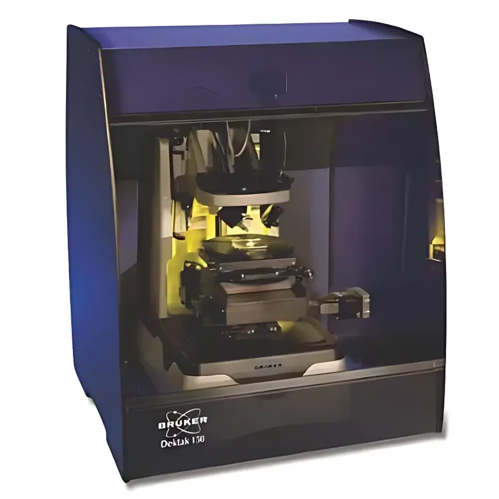
Bruker DektakXT Stylus Profilometer
| Brand | Bruker |
|---|---|
| Origin | Germany |
| Manufacturer Type | Authorized Distributor |
| Origin Category | Imported Instrument |
| Model | DektakXT |
| Price Range | USD 13,500 – 27,000 (FOB Hamburg) |
Overview
The Bruker DektakXT Stylus Profilometer is a high-precision, non-optical surface metrology instrument engineered for quantitative topographic characterization of thin films, etch depths, step heights, and surface roughness in semiconductor fabrication and advanced materials R&D. Based on contact-mode mechanical profilometry—where a diamond-tipped stylus traverses the sample surface under controlled normal force—the DektakXT delivers nanometer-level vertical resolution and sub-nanometer repeatability across lateral scales from micrometers to 100 mm. Its core measurement principle relies on high-stability linear variable differential transformer (LVDT) displacement sensing combined with precision air-bearing motion stages, enabling traceable, ISO/IEC 17025-compatible height measurements without optical diffraction limits or phase ambiguity. Designed specifically for process control in front-end-of-line (FEOL) and back-end-of-line (BEOL) semiconductor manufacturing, the system supports wafer-level inspection of photoresist development, chemical-mechanical polishing (CMP), thin-film deposition (PVD/CVD), and lithography alignment structures.
Key Features
- High-resolution vertical metrology: <0.1 nm RMS noise floor and ≤0.4 nm repeatability (1σ) over 100 µm scan range, verified per ISO 25178-6 and ASTM E1092 standards
- Automated multi-point scanning: Programmable stage with 200 mm × 200 mm travel and integrated wafer handling for 100–300 mm diameter substrates
- Diamond stylus options: Standard 2 µm radius tip (nominal force: 0.5–15 mg); optional ultra-low-force 12.5 µm radius tip for soft polymer films and low-modulus dielectrics
- Real-time signal processing: Dual-channel analog filtering, adaptive speed control, and dynamic force feedback to maintain constant tip–sample interaction during steep slope traversal
- Modular platform architecture: Compatible with vacuum-compatible stages, heated/cooled chucks (−40 °C to +150 °C), and in-situ electrochemical cells for correlative process monitoring
- Compliance-ready firmware: Audit trail logging, user access levels (admin/operator/technician), electronic signatures, and 21 CFR Part 11–compliant data export protocols
Sample Compatibility & Compliance
The DektakXT accommodates rigid and semi-rigid substrates including silicon, sapphire, SiC, GaN, quartz, fused silica, and glass wafers; patterned or unpatterned photomasks; and deposited layers such as SiO₂, SiNₓ, low-k dielectrics, metal interconnects (Al, Cu, W), and organic planarization films. It meets critical industry specifications including SEMI E10 (Specification for Definition and Measurement of Equipment Reliability and Maintainability), ISO 25178-2 (Surface texture — Areal), and ASTM B487 (Standard Test Method for Measurement of Metal and Oxide Coating Thickness by Microscopical Examination of Cross Section). All calibration artifacts are NIST-traceable, and system performance verification follows Bruker’s certified PVP (Performance Verification Protocol) procedure aligned with GLP and GMP documentation requirements.
Software & Data Management
Operating on Bruker’s proprietary Vision64 software platform, the DektakXT provides full workflow integration—from acquisition and analysis to reporting and database archiving. Vision64 supports automated recipe-based measurement sequences, statistical process control (SPC) charting (X-bar/R, Cpk), cross-sectional profile overlay, 3D surface reconstruction, and custom scripting via Python API. Raw data files (.pro) retain full metadata (timestamp, operator ID, calibration status, environmental logs), and export formats include CSV, XML, TIFF, and PDF/A-1b for long-term archival compliance. Data integrity is enforced through role-based permissions, immutable audit trails, and optional integration with enterprise LIMS or MES systems via ODBC or RESTful web services.
Applications
- Quantification of film thickness uniformity and step coverage after PECVD or ALD deposition
- Etch depth profiling in hardmask removal, trench isolation, and via formation processes
- CMP endpoint detection and post-polish dishing/erosion assessment on copper damascene structures
- Photoresist thickness mapping and development rate analysis across 300 mm wafers
- Characterization of MEMS device topography, including release etch undercut and stiction relief features
- Surface roughness validation (Sa, Sq, Sz) for EUV mask blanks and pellicle support frames
FAQ
What is the maximum measurable step height with the standard DektakXT configuration?
Standard configurations support up to 1.2 mm vertical range; extended-range modules (optional) extend this to 3.5 mm.
Can the DektakXT measure on curved or non-planar substrates?
Yes—via optional motorized tilt compensation stage and curvature correction algorithms embedded in Vision64 software.
Is the system qualified for use in Class 100 cleanroom environments?
Yes—fully compatible with ISO Class 5 (Class 100) cleanrooms when equipped with HEPA-filtered air purge and static-dissipative components.
Does Bruker provide IQ/OQ/PQ documentation packages for regulated facilities?
Yes—validated installation qualification (IQ), operational qualification (OQ), and performance qualification (PQ) protocols are available upon request and conform to FDA and EU Annex 11 requirements.
How frequently does the stylus require recalibration or replacement?
Stylus wear is monitored automatically via real-time tip radius tracking; typical service interval is 6–12 months depending on usage intensity and sample hardness.


