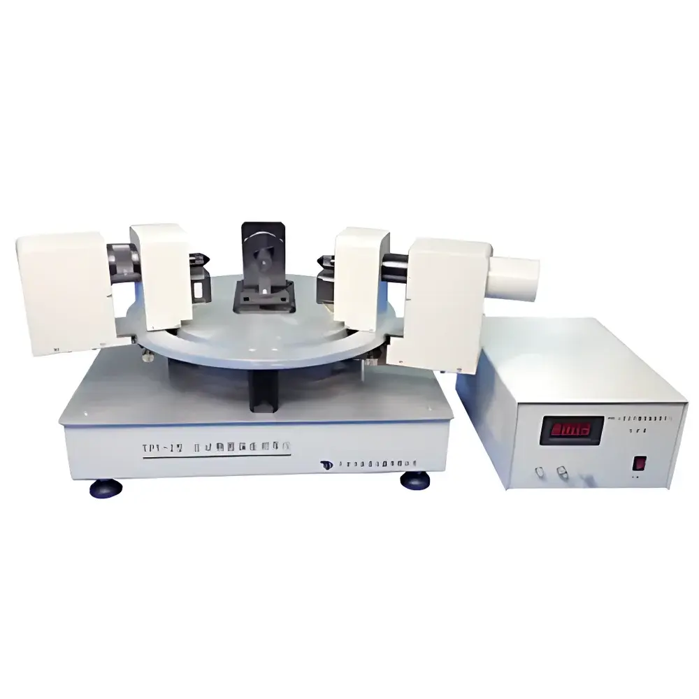
Topo TPY-2 Automatic Ellipsometer for Thin-Film Thickness and Refractive Index Measurement
| Brand | Topo |
|---|---|
| Model | TPY-2 |
| Origin | Tianjin, China |
| Manufacturer Type | Original Equipment Manufacturer (OEM) |
| Spectral Range | 632.8 nm (He–Ne laser) |
| Thickness Measurement Range | 1–4000 nm |
| Refractive Index Range | 1.0–10.0 |
| Incidence Angle Range | 20°–90° (±0.05° angular resolution) |
| Sample Diameter Compatibility | Ø10–Ø140 mm, max thickness 16 mm |
| Thickness Accuracy | ±0.5 nm (for films 10–100 nm), ±1 nm (full range) |
| Refractive Index Repeatability | ±0.005 |
| Polarizer Azimuth Range | 0°–180° |
| Optical Center Height | 80 mm |
| Dimensions (L×W×H) | 680 × 390 × 310 mm |
| Weight | 26 kg |
| Interface | USB 2.0 |
| Software | Windows-based ellipsometry analysis suite with real-time data acquisition, multi-layer modeling, and export to CSV, TXT, and XML |
Overview
The Topo TPY-2 Automatic Ellipsometer is a benchtop, null-type spectroscopic ellipsometer engineered for high-precision, non-destructive characterization of thin-film optical properties on planar substrates. It operates on the fundamental principle of ellipsometry—measuring the change in polarization state (amplitude ratio Ψ and phase difference Δ) of monochromatic light (632.8 nm He–Ne laser) upon reflection from a sample surface. By fitting measured Ψ/Δ values to physically consistent optical models—including single-layer, multi-layer, graded-index, or effective-medium approximations—the instrument quantifies film thickness and complex refractive index (n + ik) with sub-nanometer resolution. Designed for R&D laboratories and quality control environments in semiconductor fabrication, photovoltaics, optical coatings, and MEMS development, the TPY-2 delivers traceable, repeatable measurements without physical contact or vacuum requirements.
Key Features
- Null-null detection architecture using precision motorized rotating polarizer and analyzer, enabling high signal-to-noise ratio and robust baseline stability.
- Stabilized helium–neon (He–Ne) laser source (632.8 nm, <±0.002 nm wavelength drift) ensures long-term spectral fidelity and eliminates calibration drift associated with broadband sources.
- Motorized goniometer with 0.05° angular resolution and programmable incidence angle selection (20°–90°) supports angle-resolved analysis for anisotropic films and critical dimension metrology.
- Integrated USB 2.0 interface enables direct communication with Windows-based host PCs; no external DAQ cards or proprietary hardware drivers required.
- Modular optical head design accommodates optional upgrades including automated stage positioning, environmental chamber integration, or UV/Vis/NIR extension modules (not included).
- Compliance-ready architecture: software supports audit trail logging, user access levels, and electronic signature functionality aligned with GLP and ISO/IEC 17025 documentation requirements.
Sample Compatibility & Compliance
The TPY-2 accepts rigid, flat samples up to Ø140 mm in diameter and 16 mm in thickness, including silicon wafers, glass substrates, quartz plates, and metal-coated mirrors. Its fixed optical center height (80 mm) ensures compatibility with standard wafer handling fixtures and manual load locks. The system meets mechanical safety standards per IEC 61010-1 and electromagnetic compatibility (EMC) requirements per EN 61326-1. While not certified for FDA-regulated manufacturing, its measurement traceability—calibrated against NIST-traceable SiO₂/Si reference standards—and software audit capabilities support compliance with ISO 9001, ISO/IEC 17025, and internal QC protocols requiring documented uncertainty budgets.
Software & Data Management
The bundled Windows application provides a full-featured ellipsometric analysis environment: real-time Ψ/Δ monitoring, Levenberg–Marquardt nonlinear regression fitting, multi-sample batch processing, and layer stack definition with dispersion models (Cauchy, Sellmeier, Tauc–Lorentz). Raw data and fit parameters are stored in timestamped project files (.tpyproj) with embedded metadata (operator ID, date/time, instrument serial, calibration status). Export formats include CSV (for Excel or Python analysis), XML (for LIMS integration), and PDF reports compliant with internal QA templates. All software modifications are version-controlled, and configuration changes generate immutable log entries satisfying 21 CFR Part 11 “electronic records and signatures” principles for regulated users.
Applications
- Thickness mapping of SiO₂, Si₃N₄, Al₂O₃, and HfO₂ gate dielectrics in microelectronics process development.
- Optical constant determination of transparent conductive oxides (ITO, AZO) for display and solar cell applications.
- Monitoring of spin-coated polymer films (PMMA, PS) and self-assembled monolayers (SAMs) during surface functionalization studies.
- Quantification of oxidation kinetics on metal surfaces (e.g., Al, Cu) under controlled ambient exposure.
- Verification of anti-reflective and high-reflectivity coating performance in optical component manufacturing.
- Supporting ASTM F1570 (Standard Test Method for Thickness of Transparent Films Using Spectroscopic Ellipsometry) and ISO 15382 (Thin film thickness measurement by ellipsometry).
FAQ
What type of light source does the TPY-2 use, and why is it advantageous?
The TPY-2 employs a stabilized helium–neon (He–Ne) laser at 632.8 nm. This monochromatic source provides superior wavelength stability (<±0.002 nm), eliminating spectral broadening artifacts common in LED or halogen-based systems—critical for resolving ultra-thin films (<5 nm) where small Δ shifts dominate sensitivity.
Can the TPY-2 measure multilayer stacks?
Yes. The software includes a hierarchical optical model builder supporting up to five discrete layers, each with independently variable n(k), thickness, and roughness parameters. Users may constrain or decouple variables based on prior knowledge (e.g., fixed substrate n, known top-layer k).
Is vacuum operation required?
No. The TPY-2 operates in ambient air. For measurements sensitive to surface adsorption (e.g., hydrocarbon contamination on ultrathin oxides), optional dry nitrogen purge or glovebox integration is supported via auxiliary gas ports.
How is measurement uncertainty quantified?
Uncertainty is derived from Type A (repeatability: 0.5 nm thickness, 0.005 n) and Type B (calibration standard uncertainty, angular encoder resolution, laser wavelength tolerance) components per GUM (JCGM 100:2008). Full uncertainty budgets are auto-generated in exported reports.
Does the system support automated stage scanning?
The base configuration includes manual XY stage adjustment. Motorized XYZ translation stages and programmable wafer mapping are available as factory-installed options (TPY-2-MAP), enabling spatial uniformity analysis across 150-mm wafers.


