DENSsolutions Lightning In Situ TEM Heating & Electrical Biasing System
| Brand | DENSsolutions |
|---|---|
| Origin | Netherlands |
| Model | Lightning |
| Temperature Range | RT–1300 °C |
| Displacement Resolution | < 200 nm |
| Tensile Rate | ≤ 0.5 nm/min |
Overview
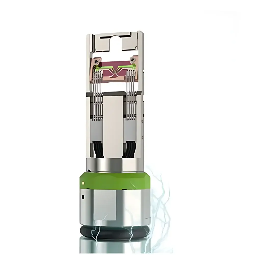
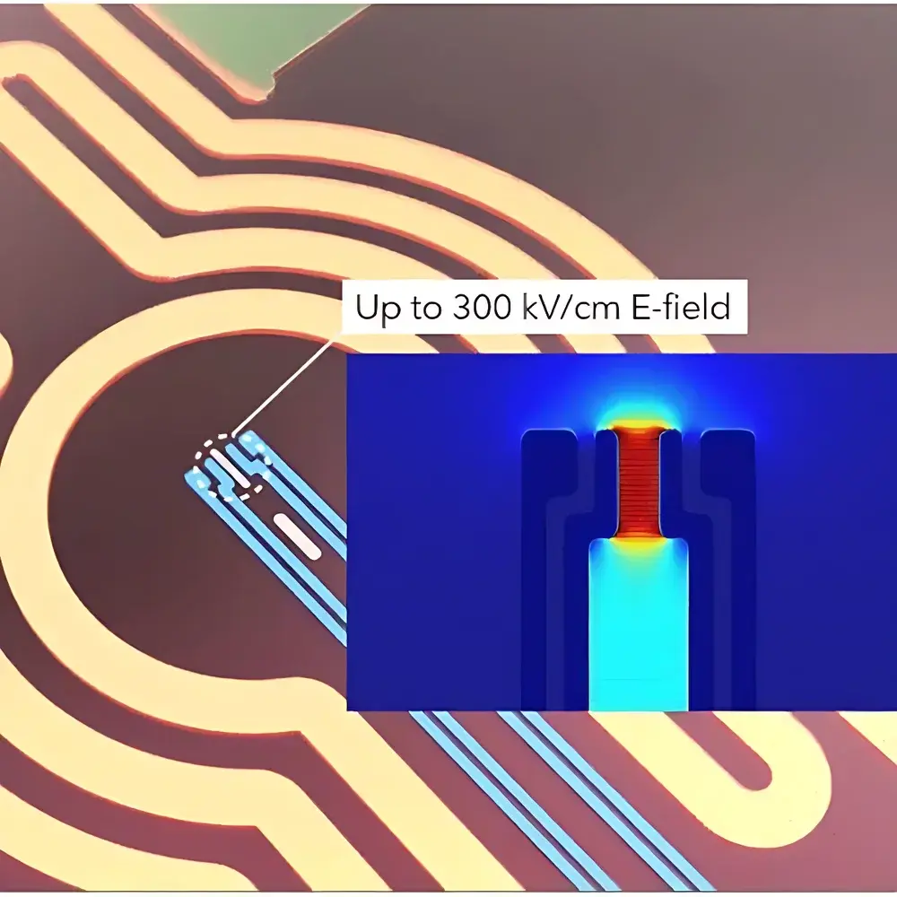
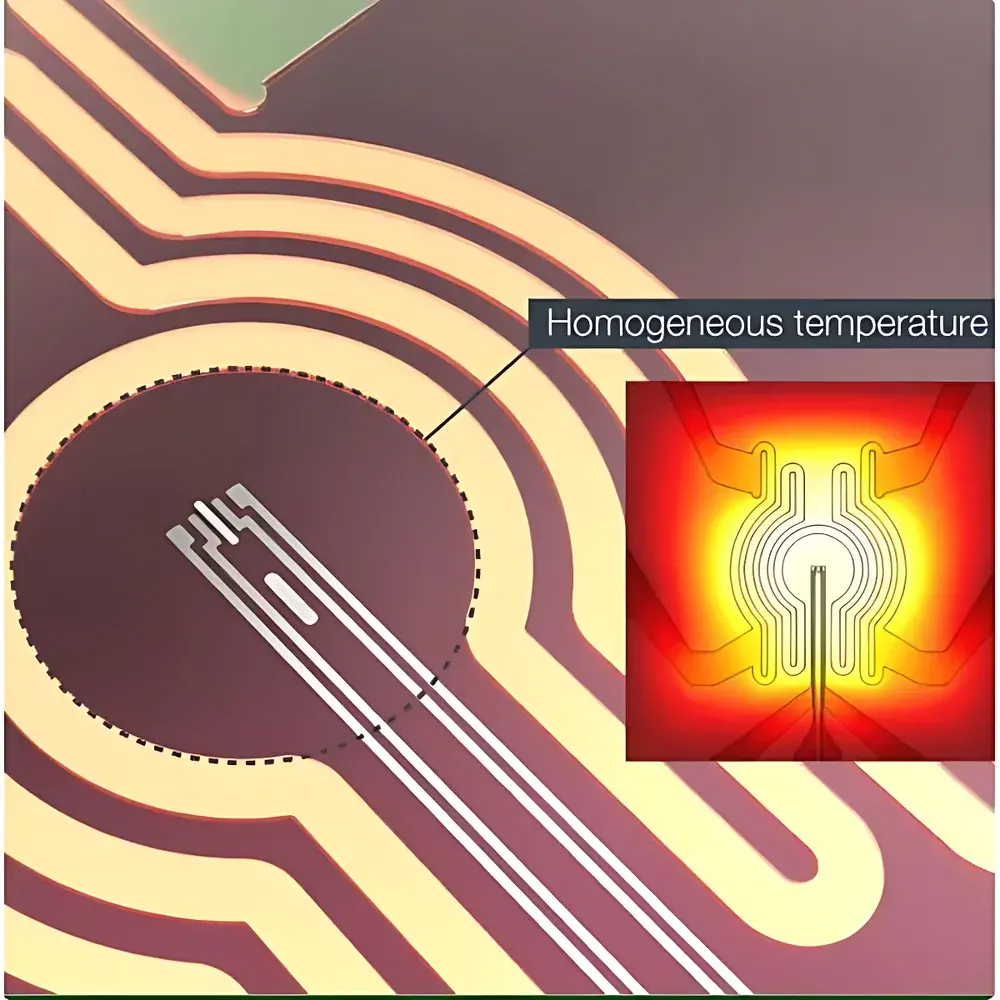
The DENSsolutions Lightning In Situ TEM Heating & Electrical Biasing System is an advanced MEMS-based platform engineered for simultaneous, independent, and precisely controlled thermal and electrical stimulation inside high-resolution transmission electron microscopes (TEM/STEM). Unlike conventional in situ holders that compromise resolution under stimulus, the Lightning system leverages proprietary Nano-Chip technology to maintain atomic-scale imaging fidelity while delivering calibrated heating up to 1300 °C and electric fields exceeding 300 kV/cm—enabling real-time observation of dynamic structural, phase, and electronic responses under technologically relevant operating conditions. Its core architecture integrates four-terminal sensing for drift-compensated voltage/current control and direct in-chamber temperature validation via EELS and SAED, ensuring metrological traceability without post-acquisition correction. Designed for compatibility with 200–300 kV TEMs—including aberration-corrected systems—the Lightning system extends TEM from static characterization to quantitative, stimulus-synchronized operando analysis.
Key Features
- Atomic-Resolution Stability Under Stimulus: Achieves sub-200 nm mechanical drift over ΔT = 1000 °C; Z-axis thermal expansion is actively minimized and decoupled from imaging axis, preserving diffraction-limited resolution during heating and biasing.
- True pA-Level Current Sensitivity: Integrated low-noise electronics enable concurrent I–V characterization at picoampere sensitivity while acquiring HRTEM or STEM images—critical for correlating electronic transport with nanoscale structural evolution.
- MEMS Nano-Chip Flexibility: Interchangeable chips support multiple configurations (e.g., 2-probe, 4-probe, dual-heater, asymmetric electrode layouts), each fabricated using ultra-thin SiN membranes (< 50 nm) to maximize electron transparency and thermal responsiveness.
- FIB-Compatible Sample Preparation: Optimized workflow allows final FIB thinning directly on the Nano-Chip, eliminating transfer-induced contamination or damage and maintaining chip functionality post-preparation.
- In-Situ Temperature Metrology: On-chip Pt resistance thermometry cross-validated by EELS plasmon shift and SAED lattice parameter calibration ensures ±5 °C accuracy across the full RT–1300 °C range.
Sample Compatibility & Compliance
The Lightning system accommodates standard 3-mm TEM half-grid geometries and supports both bulk and lamella specimens prepared via FIB-SEM. It complies with ISO 14644-1 Class 5 cleanroom handling protocols for chip loading and meets vacuum compatibility requirements for UHV TEM columns (≤1×10⁻⁸ mbar base pressure). All electrical interfaces are galvanically isolated and rated for continuous operation at 100 V DC bias; thermal management conforms to IEC 61000-4-2 ESD immunity standards. The system is routinely deployed in GLP-compliant labs performing materials qualification per ASTM E2931 (in situ TEM methodology) and supports audit-ready data logging aligned with FDA 21 CFR Part 11 requirements when paired with DENSsolutions’ certified software suite.
Software & Data Management
Control and synchronization are managed through the DENSsolutions Control Software (v5.2+), a Windows-based application providing closed-loop PID regulation of temperature and voltage, real-time current/voltage logging at 10 kHz sampling, and hardware-triggered acquisition coupling with Gatan, TVIPS, or Direct Electron detectors. All experimental parameters—including setpoints, sensor readings, and timestamped metadata—are embedded in TIFF/EMD file headers, ensuring FAIR (Findable, Accessible, Interoperable, Reusable) data provenance. Export modules support HDF5 and MRC formats for integration into Python-based analysis pipelines (e.g., HyperSpy, Atomap) and machine learning workflows. Audit trails record user actions, parameter changes, and system health diagnostics—fully compliant with laboratory information management system (LIMS) integration.
Applications
- Real-time observation of electromigration-driven void nucleation and grain boundary sliding in interconnect metallization at >800 °C
- In situ I–V spectroscopy of resistive switching in transition metal oxides during thermal cycling (RT → 1000 °C)
- Atomic-scale tracking of phase segregation kinetics in core–shell nanoparticles under coupled thermal–electrical stress
- Quantitative measurement of thermal expansion coefficients and interfacial strain relaxation in heterostructured 2D materials
- Operando study of solid-electrolyte interphase (SEI) formation on battery electrode materials under applied bias and elevated temperature
FAQ
Is the Lightning system compatible with spherical aberration-corrected (Cs-corrected) TEMs?
Yes—it maintains <0.1 nm probe stability at 300 kV under full thermal–electrical load, verified by long-duration atomic column tracking in SrTiO3 and graphene.
Can temperature and voltage be ramped independently and simultaneously?
Yes—four-terminal architecture enables fully decoupled control; arbitrary waveforms (linear ramps, step functions, sinusoidal modulation) can be programmed for either stimulus with synchronized detector triggering.
What vacuum requirements must the TEM column meet?
The holder operates stably down to 1×10⁻⁸ mbar; outgassing rates are <1×10⁻¹¹ Pa·m3/s per chip, validated per ISO 14000-17.
How is electrical noise mitigated during high-sensitivity pA measurements?
Shielded coaxial cabling, differential signal conditioning, and active guarding reduce broadband noise to <10 fA/√Hz at 1 Hz, enabling reliable single-electron-event detection in low-conductance nanowires.
Are custom Nano-Chip designs available for proprietary experimental geometries?
Yes—DENSsolutions offers collaborative chip co-design services under NDA, including bespoke electrode patterning, integrated thermocouples, and multi-zone heater layouts.


