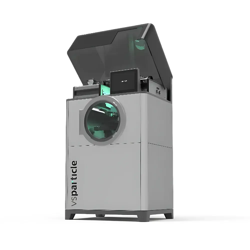
VSParticle VSP-P1 Aerosol Inkjet Printing Deposition System
| Brand | VSParticle |
|---|---|
| Origin | Netherlands |
| Model | VSP-P1 |
| Target Materials | Conductive metals and alloys |
| Substrate Size | 10 mm (monodisperse deposition), 47 mm (filter-based deposition) |
| Substrate Temperature | Ambient (~25 °C) |
| Film Thickness Uniformity | 0–20 nm (monodisperse nanoparticle deposition) |
| Base Pressure | 0.8–1.2 bar (note: this is *absolute pressure*, not vacuum level |
Overview
The VSParticle VSP-P1 Aerosol Inkjet Printing Deposition System is a benchtop nanoscale patterning platform engineered for direct-write, additive manufacturing of functional nanostructured thin films. Unlike conventional physical vapor deposition (PVD) or solution-based printing methods, the VSP-P1 employs spark ablation–generated aerosol nanoparticles transported in inert carrier gas and deposited via controlled aerodynamic impaction under low-pressure (<10 mbar) conditions. This process—termed Aerosol Impaction Printing (AIP)—enables dry, solvent-free, one-step fabrication of high-purity metallic, alloy, and metal oxide nanostructures with preserved native crystallinity and surface chemistry. The system operates without binders, ligands, or post-deposition thermal annealing, making it uniquely suited for thermally sensitive substrates (e.g., polymers, flexible electronics) and applications requiring pristine nanomaterial interfaces—such as electrocatalysis, plasmonic sensing, and chemiresistive gas detection.
Key Features
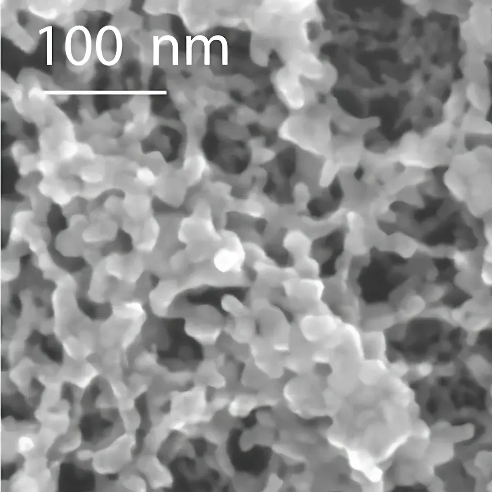
- Spark ablation-based aerosol generation: Enables in situ synthesis of monodisperse, ligand-free nanoparticles (0–20 nm) from bulk conductive targets—including pure metals (Au, Ag, Ni, Fe, Cu), binary/alloy systems (NiFe, CoCu), and metal oxides (SnO₂, ZnO, WO₃).
- Modular aerosol generator: Detachable spark ablation module supports independent nanoparticle synthesis studies, cross-platform integration (e.g., with TEM grids or electrochemical cells), and rapid target exchange.
- Precision XYZ motion control: High-resolution linear stages (±0.5 µm repeatability) enable sub-100 µm feature definition and programmable multi-channel deposition patterns.
- Ambient-temperature substrate processing: No heating stage required; compatible with PET, PI, paper, and other low-Tg substrates.
- Low-pressure deposition chamber: Maintains dynamic pressure <10 mbar during operation—ensuring laminar aerosol flow, minimized particle agglomeration, and enhanced spatial resolution.
- Minimal waste & zero solvents: No ink formulation, no developer, no rinse steps—reducing chemical inventory, disposal burden, and contamination risk.
Sample Compatibility & Compliance
The VSP-P1 accommodates standard circular substrates up to 47 mm diameter (filter-based collection) or 10 mm diameter (high-resolution monodisperse patterning). It supports rigid (Si/SiO₂ wafers, glass slides) and flexible (polyimide, PET, aluminum foil) substrates without clamping-induced deformation. All wetted components are electropolished stainless steel or PTFE-lined; gas pathways are compatible with Ar, He, and N₂ carrier gases. The system conforms to CE marking requirements for laboratory equipment (2014/30/EU EMC Directive, 2014/35/EU LVD). While not certified for cleanroom Class 100 operation, its closed aerosol path and filtered exhaust minimize particulate release—supporting ISO 14644-1 compliant integration when installed with local ventilation.
Software & Data Management
Control is executed via VSP-Studio—a Windows-based application supporting G-code-compatible trajectory programming, real-time pressure monitoring (capacitance manometer), and synchronized spark pulse logging. All deposition parameters (spark frequency, carrier gas flow, stage velocity, dwell time per pixel) are timestamped and stored in HDF5 format for traceability. Export options include CSV (process metadata), TIFF (pattern mask overlays), and JSON (machine state snapshots). Audit trails comply with GLP-aligned documentation practices; raw data files retain unaltered sensor timestamps and user annotations—facilitating FDA 21 CFR Part 11–compatible validation protocols when paired with institutional electronic lab notebook (ELN) systems.
Applications
- High-throughput electrocatalyst screening: Rapid deposition of 64+ composition-gradient NiFe anodes on carbon paper enables kinetic evaluation at industrially relevant current densities (>100 mA/cm²) under flow-cell conditions—accelerating catalyst optimization without binder-induced mass transport artifacts.
- SERS substrate fabrication: Direct-write of fractal Au/Ag nanoparticle arrays yields reproducible electromagnetic hotspots. Demonstrated enhancement factors >10⁷ for Rhodamine 6G, p-MBA, and melamine—without organic residue interference common in colloidal lithography.
- MOX gas sensor prototyping: Room-temperature deposition of porous SnO₂ and WO₃ films preserves stoichiometry and grain boundary density critical for O₂ adsorption kinetics—eliminating post-annealing-induced phase segregation observed in sputtered or sol-gel-derived equivalents.
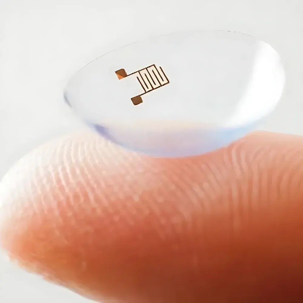
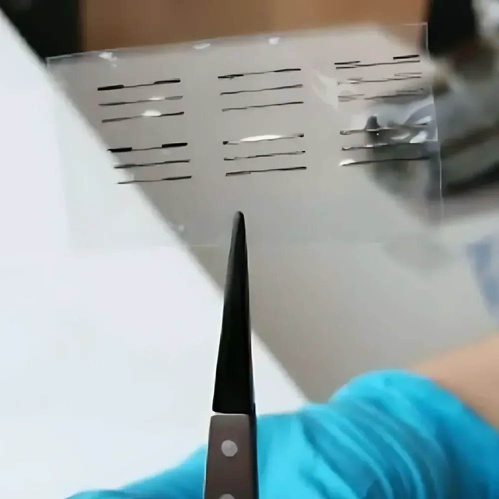
- Flexible hybrid electronics: Integration of Ag nanoparticle interconnects with printed organic semiconductors (e.g., P3HT:PCBM) on PET substrates—achieving sheet resistances <50 Ω/sq without substrate warping or interlayer diffusion.
FAQ
What nanoparticle size distribution does the VSP-P1 achieve?
Monodisperse mode yields primary particles with geometric standard deviation (σg) <1.25 and median diameter tunable between 2 nm and 20 nm—verified by inline SMPS and offline TEM analysis.
Can the system deposit insulating materials like Al₂O₃ or SiO₂?
Yes—using electrically conductive composite targets (e.g., Al–Al₂O₃ sintered pellets) or pulsed DC spark ablation of doped ceramic rods; stoichiometry is preserved in the as-deposited film.
Is remote operation supported?
VSP-Studio includes TCP/IP API access for Python- and LabVIEW-based automation; SSH tunneling enables secure off-site monitoring and script-triggered deposition sequences.
What maintenance intervals are recommended?
Spark electrodes require replacement every ~200 hours of cumulative ablation time; carrier gas filters are rated for 6 months under continuous use; vacuum pump oil should be changed quarterly per manufacturer specifications.
How is pattern registration accuracy ensured across multiple layers?
Integrated optical encoder feedback on all axes provides closed-loop positioning; optional USB microscope module (sold separately) enables fiducial-based alignment with ±2 µm overlay tolerance.


