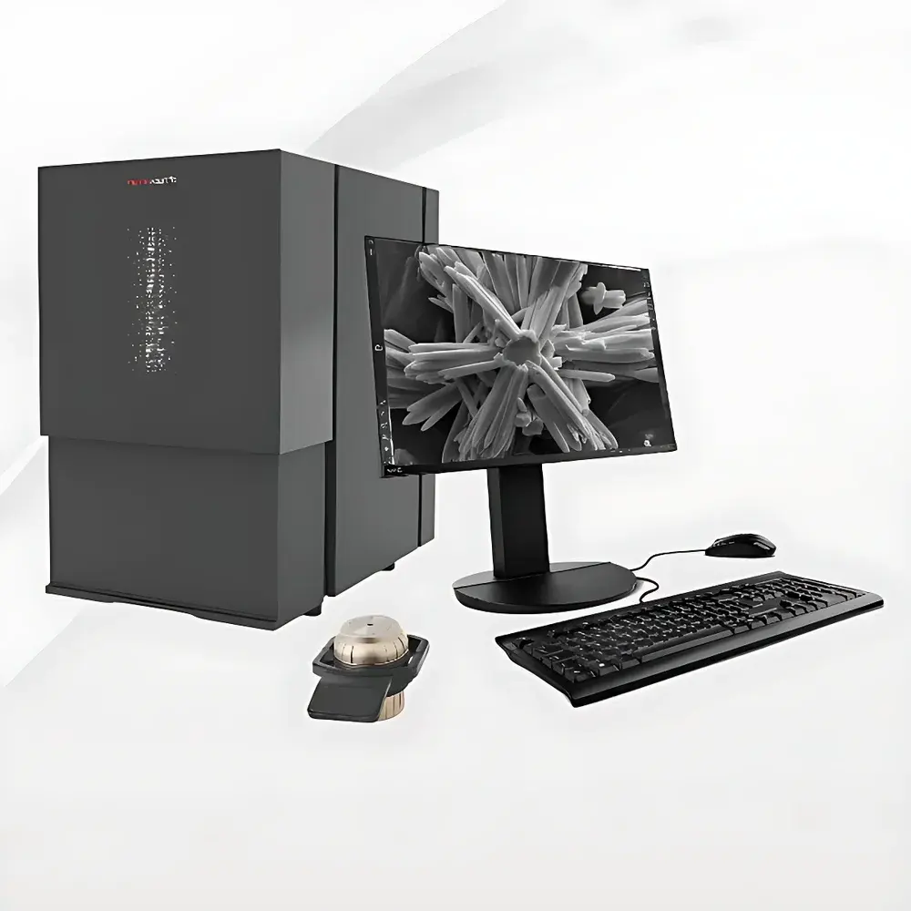
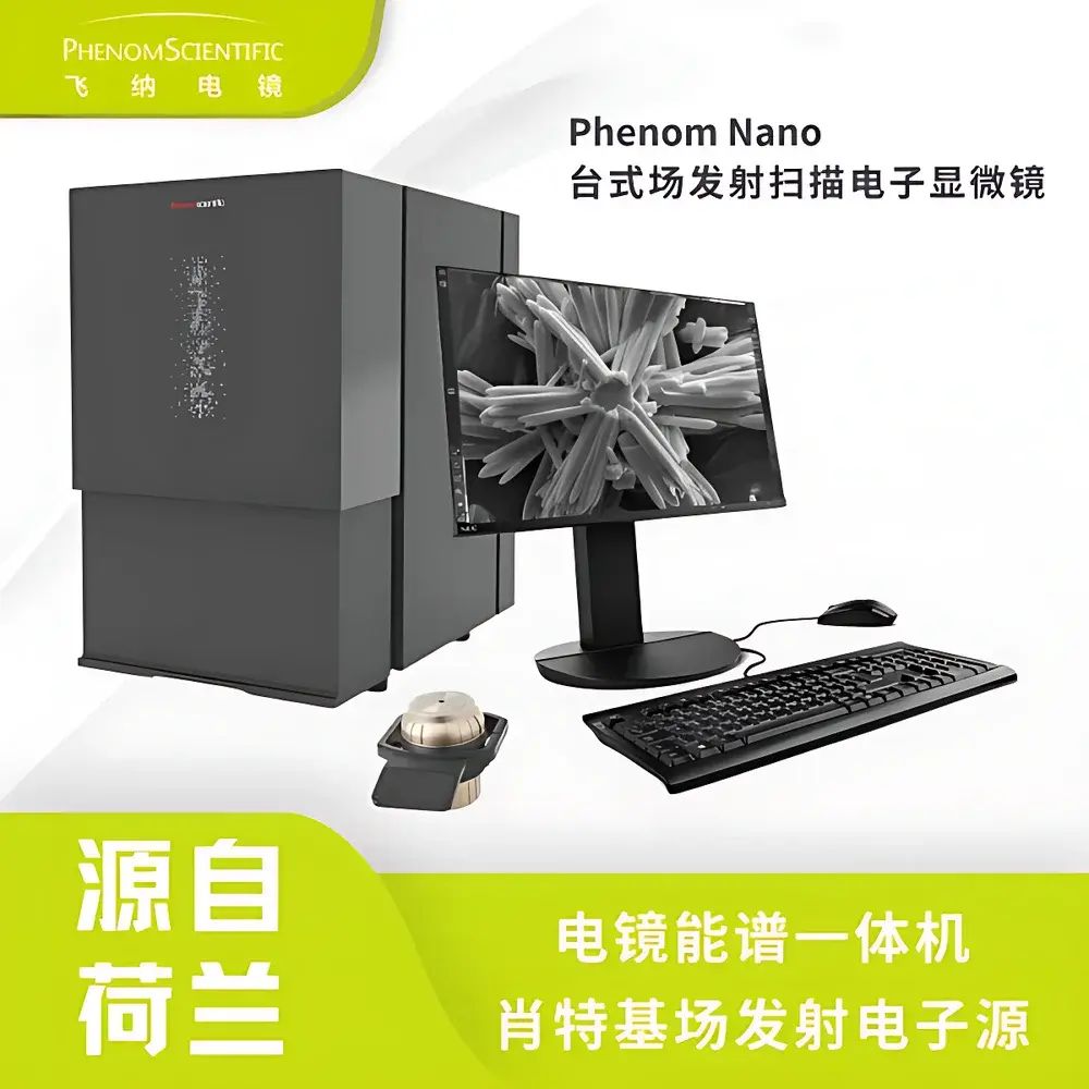
Phenom Nano G2 Desktop Field-Emission Scanning Electron Microscope
| Brand | Phenom |
|---|---|
| Origin | Netherlands |
| Manufacturer | Thermo Fisher Scientific (Phenom brand) |
| Type | Desktop SEM |
| Electron Source | Schottky Field-Emission |
| Imaging Modes | Secondary Electron (SE) & Backscattered Electron (BSE) |
| SE Resolution | ≤2.5 nm @ 15 kV |
| BSE Resolution | ≤2.5 nm @ 15 kV |
| Max Magnification | 1,000,000× |
| Vacuum Cycle Time | <15 s |
| Sample Compatibility | Conductive & Non-conductive (uncoated), Magnetic |
| Navigation | Integrated Color Optical Microscope with Panoramic View |
| Stage | Motorized XYZ Stage with Auto-Align |
| Vibration Isolation | Built-in 27-Element Passive Damping System |
| Maintenance | Field-Emission Source Lifetime >2,000 h |
Overview
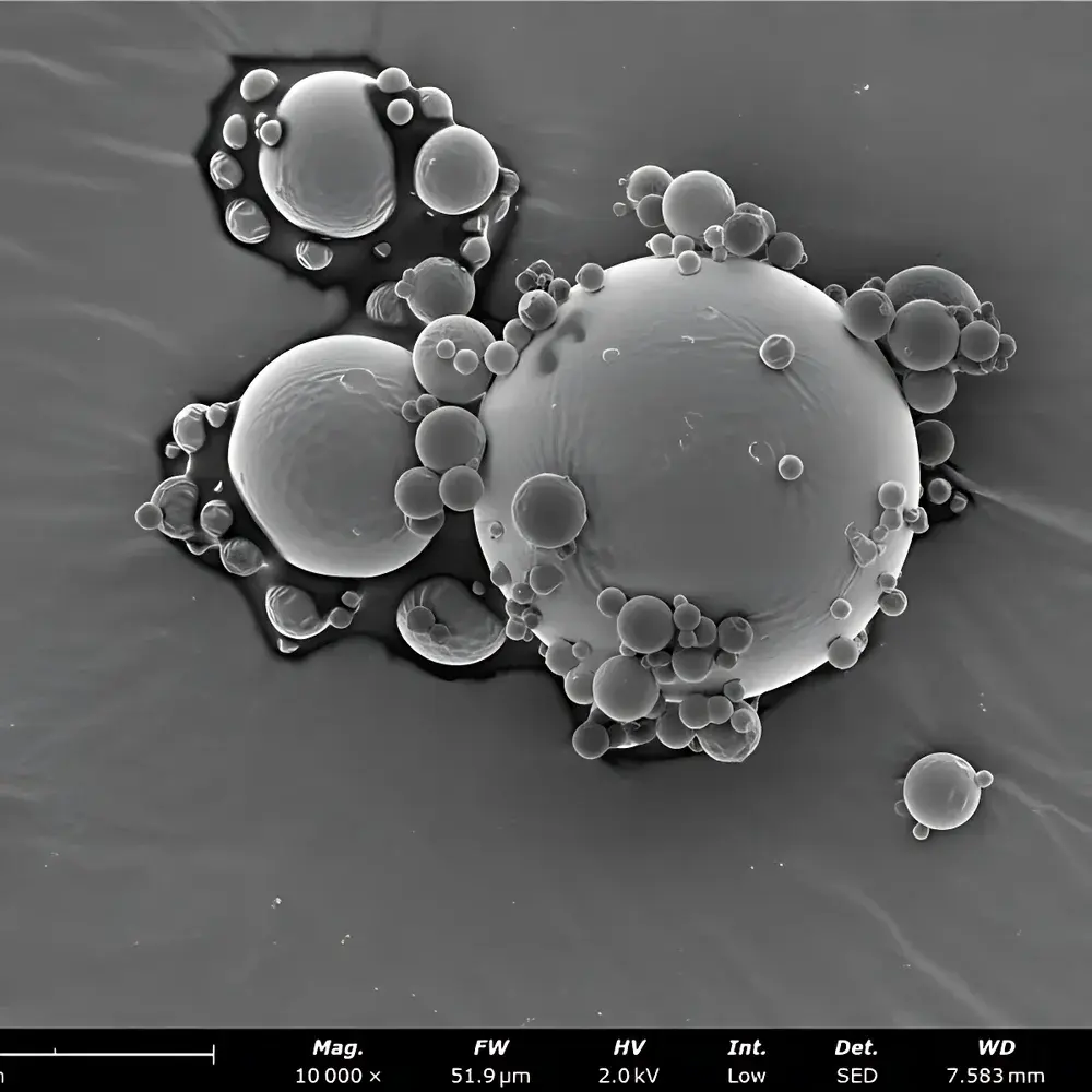
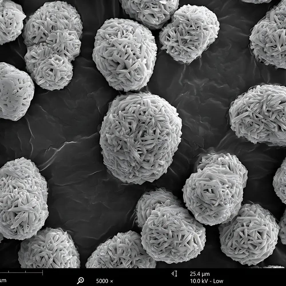
The Phenom Nano G2 is a high-performance desktop field-emission scanning electron microscope (FE-SEM) engineered for nanoscale imaging, compositional analysis, and routine materials characterization in academic laboratories, quality control environments, and industrial R&D settings. Unlike conventional floor-standing SEMs, the Nano G2 integrates a high-brightness Schottky field-emission electron source into a compact, fully shielded benchtop platform—delivering sub-2.5 nm resolution at 15 kV without requiring cryogenic cooling or ultra-high vacuum infrastructure. Its operational principle relies on thermally assisted field emission from a zirconium-oxide-coated tungsten tip, enabling stable beam current, low energy spread (<0.8 eV), and exceptional signal-to-noise ratio across magnifications from 10× to 1,000,000×. The system employs a coaxial electron optical column with optimized electromagnetic lens design, minimizing spherical and chromatic aberrations while maintaining consistent probe convergence across accelerating voltages (5–15 kV). This architecture supports simultaneous acquisition of secondary electron (SE) and backscattered electron (BSE) signals—enabling topographic contrast, atomic number contrast, and phase differentiation without sample coating.
Key Features
- Sub-2.5 nm resolution imaging in both SE and BSE modes at 15 kV—validated per ISO 16700:2016 test protocols
- Integrated full-color optical microscope with 4×–100× zoom and panoramic stitching for rapid region-of-interest navigation
- Motorized XYZ stage with 50 mm × 50 mm travel range and automated tilt/rotation alignment for multi-angle imaging
- Patented 15-second vacuum cycle enabled by dual-stage turbomolecular pumping and leak-tight ceramic vacuum chamber
- No-coating operation for insulating samples (e.g., polymers, ceramics, biological tissues) via low-kV imaging and charge compensation mode
- Magnetic sample compatibility ensured by zero-residual-field design—no magnetic shielding required for ferromagnetic specimens
- Passive vibration isolation using 27 independent elastomeric damping elements compliant with ISO 25317:2013 mechanical stability requirements
- Sealed electron optics path with lifetime-rated Schottky emitter (>2,000 h mean time between failures)
Sample Compatibility & Compliance
The Phenom Nano G2 accommodates samples up to 100 mm in diameter and 50 mm in height—including bulk metals, semiconductor wafers, geological sections, electrospun fibers, freeze-dried biomaterials, and uncoated printed circuit boards. Its charge-neutralization capability eliminates the need for conductive sputter coating, preserving native surface chemistry for subsequent EDS analysis. The instrument complies with IEC 61000-6-3 (EMC emissions), IEC 61000-6-2 (immunity), and meets essential safety requirements under EU Directive 2014/30/EU (EMC) and 2014/35/EU (LVD). For regulated environments, optional audit-trail-enabled software supports 21 CFR Part 11 compliance when paired with validated EDS modules and networked data storage solutions.
Software & Data Management
Operation is managed through Phenom Desktop Software v5.x—a Windows-based interface supporting automated workflow scripting, batch image acquisition, and real-time drift correction. All acquired images embed EXIF metadata (kV, WD, dwell time, detector gain, stage coordinates), ensuring traceability per ISO/IEC 17025:2017 documentation requirements. Raw TIFF and HDF5 export formats enable third-party processing in MATLAB, Python (scikit-image), or commercial packages such as DigitalMicrograph. Remote diagnostics and firmware updates are delivered securely over TLS 1.2–encrypted connections; Thermo Fisher provides lifetime remote support access without recurring subscription fees.
Applications
The Nano G2 serves critical roles in failure analysis of microelectronics packaging, particle size distribution quantification in pharmaceutical dry powder inhalers (per USP ), pore structure evaluation in battery electrode coatings, fracture surface morphology assessment in aerospace alloys (ASTM E3-22), and nanofiber diameter statistics in filtration media development. Its rapid turnaround time (<90 s from load to first image) makes it suitable for inline QC in additive manufacturing facilities, where layer adhesion defects and powder morphology deviations must be assessed per ASTM F3122-21.
FAQ
Does the Phenom Nano G2 require liquid nitrogen or external water cooling?
No. The Schottky emitter operates at ~1,800 K and is air-cooled via integrated heat pipes and convection fins—eliminating cryogen dependency.
Can the system perform elemental mapping without an external EDS detector?
The Nano G2 platform is compatible with optional integrated silicon drift detector (SDD) modules; standalone imaging does not include EDS, but the vacuum and stage interfaces are pre-configured for seamless upgrade.
What vacuum level is achieved during operation?
The chamber reaches ≤5 × 10⁻⁷ mbar within 15 seconds using a 80 L/s turbomolecular pump backed by a dry scroll pump—meeting SEM operational specifications per ISO 12197-1:2019.
Is training required to operate the instrument independently?
Yes—30 minutes of guided instruction covers loading, focus optimization, contrast adjustment, and basic measurement tools; no prior SEM experience is assumed.
How is long-term calibration maintained?
The system includes automated pixel size calibration using certified NIST-traceable grating standards; all geometric corrections are applied in real time during acquisition.


