Phenom Automated Image Mapping Module for Desktop SEM
| Brand | Phenom |
|---|---|
| Origin | Netherlands |
| Manufacturer Type | Authorized Distributor |
| Product Origin | Imported |
| Model | Automated Image Mapping |
| Pricing | Available Upon Request |
| Max Scan Area | 100 mm × 100 mm |
| Imaging Modes | Backscattered Electron (BSE), Secondary Electron (SE) |
| Focus Mode | Auto-focus |
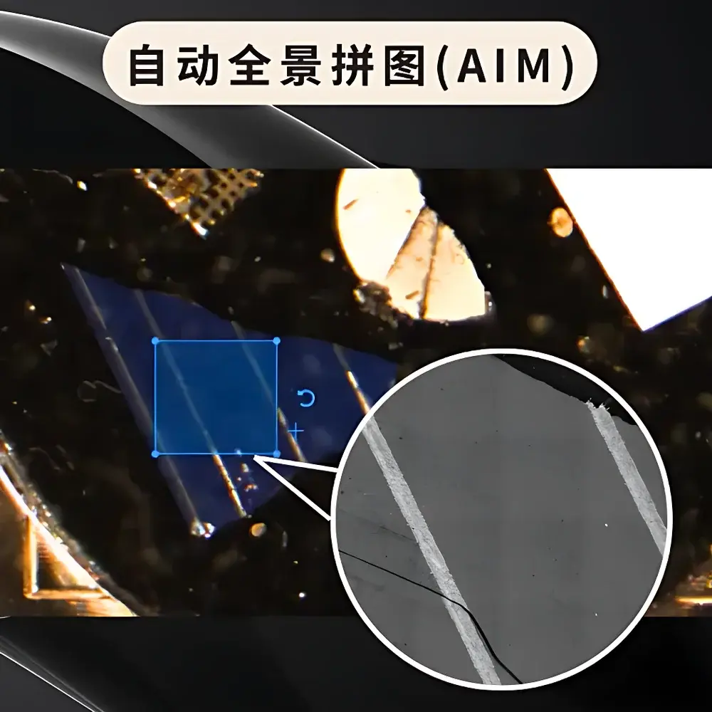
| Stitching | Fully Automated, Sub-pixel Registration |
| Stage Control | High-precision Motorized XY Stage |
| UI | Integrated Touch-Optimized Interface |
| Compatible With | Phenom Desktop SEM Series (e.g., Phenom XL, Phenom Pharos, Phenom Pure) |
Overview
The Phenom Automated Image Mapping Module is a purpose-built software-hardware integration solution designed exclusively for Phenom desktop scanning electron microscopes (SEM). It addresses a fundamental limitation in conventional SEM imaging: the trade-off between field-of-view and resolution when characterizing large or irregularly shaped specimens. Leveraging the Phenom platform’s high-brightness CeB₆ electron source, precision motorized XY stage with sub-micron repeatability, and real-time image alignment algorithms, this module enables automated acquisition and seamless stitching of multi-frame electron images into a single, geometrically coherent panoramic map—without requiring manual stage repositioning, external scripting, or post-acquisition third-party software. The system operates natively within the Phenom user interface, ensuring full synchronization with beam control, detector settings, and vacuum status. It is engineered for laboratories where rapid contextual assessment—such as fracture surface mapping, PCB defect localization, or tissue-level morphology survey—is required prior to high-magnification targeted analysis.
Key Features
- Fully integrated, touch-optimized UI embedded directly in the Phenom operating system—no external PC or software installation required.
- Customizable scan region definition via freehand polygon drawing or rectangular/elliptical ROI selection—minimizing unnecessary data acquisition and storage overhead.
- Dynamic field-of-view adjustment: users can select nominal magnifications from 20× to 10,000× per tile, with continuous interpolation across the range.
- Hardware-synchronized auto-focus at each tile position—critical for samples exhibiting >100 µm topographic variation, such as cast metals or freeze-fractured biological sections.
- Sub-pixel image registration using feature-based cross-correlation and intensity gradient matching—ensuring <0.5 µm positional accuracy between adjacent tiles.
- Real-time stitching preview during acquisition; final mosaic exported in TIFF (16-bit), PNG, or Phenom-native .pim format with embedded scale bar and metadata (date, operator, instrument ID, kV, WD, detector type).
Sample Compatibility & Compliance
The module supports conductive and non-conductive specimens up to 100 mm × 100 mm in footprint and ≤50 mm in height (subject to Phenom chamber constraints). Standard stubs, petri dishes, silicon wafers, metallographic mounts, and SEM-compatible microscope slides are routinely imaged without modification. For non-conductive samples, standard carbon or Au/Pd sputter coating remains recommended. The system complies with IEC 61000-6-3 (EMC emissions) and IEC 61000-6-2 (immunity), and its software architecture supports audit trail generation per ISO/IEC 17025:2017 Clause 7.8.2 for accredited testing laboratories. While not FDA-cleared as a medical device, it meets general-purpose instrumentation requirements under ISO 13485–aligned quality management systems used in R&D and QC environments.
Software & Data Management
Image mapping workflows are managed through Phenom’s proprietary software suite, which logs all acquisition parameters—including tile count, dwell time, pixel size (down to 1.5 nm/pixel at 10,000×), total scan time, and stage coordinates—in a structured XML metadata header. Exported mosaics retain calibrated spatial information compatible with open-source tools (e.g., Fiji/ImageJ) and commercial platforms (e.g., Thermo Scientific Avizo, Olympus Stream). Batch processing of multiple maps—including contrast normalization, annotation overlay, and region-of-interest (ROI) area quantification—is supported via scriptable API access (Python SDK available under NDA). All user actions—including ROI drawing, focus initiation, and export—are timestamped and traceable for GLP/GMP-aligned documentation.
Applications
- Fractography: Correlating macro-scale crack propagation paths with local microstructural features (e.g., inclusion clusters, grain boundary decohesion) across entire fracture surfaces.
- PCB & Microelectronics Failure Analysis: Rapid localization of solder joint voids, trace delamination, or contamination zones on full-board assemblies prior to FIB-SEM cross-sectioning.
- Metallurgy & Materials Science: Documenting heat-affected zones, weld bead geometry, and phase distribution in large-section metallographic samples.
- Life Sciences: Survey imaging of cultured cell monolayers, histological sections, or insect exoskeletons—preserving spatial context while enabling subsequent high-resolution sub-area navigation.
- Geosciences & Forensics: Mapping mineralogical heterogeneity in thin sections or particle distribution in soil/sediment samples at mm-to-µm scale continuity.
FAQ
Is the Automated Image Mapping Module compatible with all Phenom SEM models?
Yes—it is validated for Phenom XL, Phenom Pharos, and Phenom Pure systems equipped with firmware version 4.12 or later.
Does panoramic stitching require user intervention during acquisition?
No—tile acquisition, autofocus, stage movement, and real-time alignment are fully autonomous once the ROI and magnification are defined.
Can stitched images be used for quantitative measurements?
Yes—calibrated pixel size is preserved throughout the mosaic; measurement tools (line, angle, area) function identically as in single-frame imaging.
What is the maximum file size for a 100 mm × 100 mm map at 10 nm/pixel resolution?
Approximately 10–12 GB for a 16-bit TIFF, depending on compression settings and tile overlap; SSD-based internal storage is recommended.
Is offline stitching supported for legacy acquisitions?
No—stitching is tightly coupled to hardware synchronization; only maps acquired using this module’s native workflow are supported.


