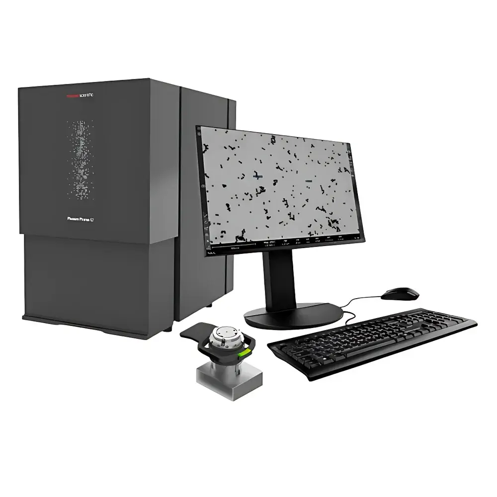
Phenom Pharos-STEM Desktop Field-Emission Scanning Transmission Electron Microscope
| Brand | Phenom |
|---|---|
| Origin | Netherlands |
| Manufacturer Type | Original Equipment Manufacturer (OEM) |
| Origin Category | Imported |
| Model | Pharos-STEM |
| Pricing | Available Upon Request |
Overview
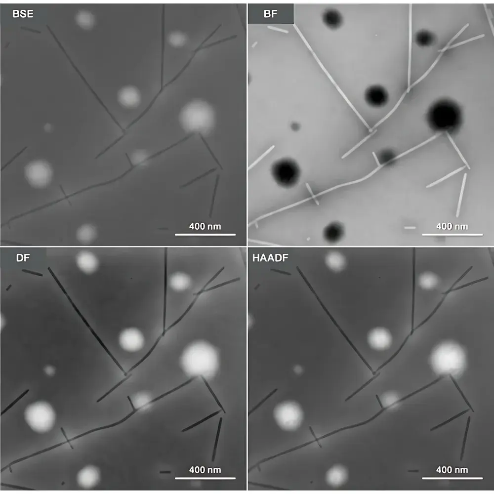
The Phenom Pharos-STEM is a uniquely engineered desktop field-emission scanning transmission electron microscope (STEM), designed to bridge the performance gap between conventional benchtop SEMs and full-scale TEM systems. Unlike traditional transmission imaging requiring high-voltage (≥100 kV) vacuum column architectures, the Pharos-STEM operates at accelerating voltages from 1–20 kV using a cold field-emission gun (FEG), enabling high-resolution STEM imaging with significantly reduced beam-induced damage—particularly critical for beam-sensitive materials such as polymers, biological macromolecules, hydrated specimens, and soft nanomaterials. Its integrated STEM detection system captures transmitted electrons through three complementary modalities: Bright-Field (BF), Dark-Field (DF), and High-Angle Annular Dark-Field (HAADF), each governed by distinct scattering physics and detector geometry. BF imaging relies on coaxial collection of unscattered and low-angle scattered electrons, delivering thickness- and composition-dependent contrast ideal for low-Z element visualization. DF mode employs off-axis detectors to emphasize diffracted or elastically scattered electrons, enhancing crystallinity and phase boundary contrast. HAADF imaging utilizes high-angle incoherent Rutherford scattering, producing Z-contrast images where signal intensity scales approximately with Z²—making it highly sensitive to heavy atoms within light matrices. This multi-modal capability is embedded within a fully automated, vacuum-integrated platform compatible exclusively with the Phenom Pharos G2 desktop FEG-SEM base system.
Key Features
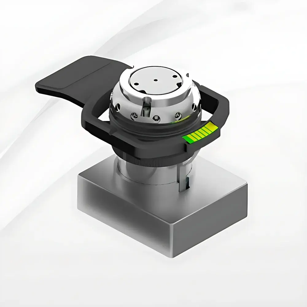
- Integrated STEM detection module with 11-segment annular detector array for fully customizable signal acquisition
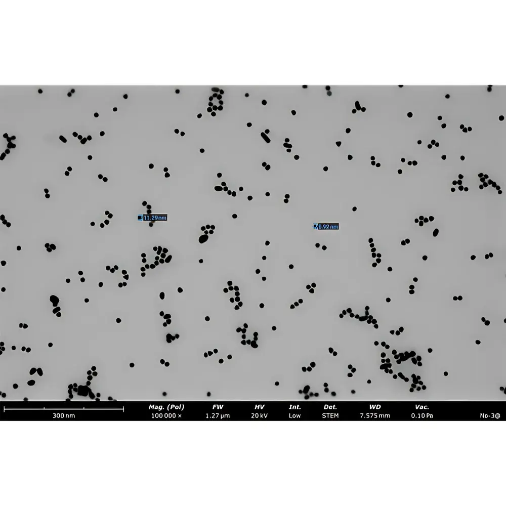
- Cold field-emission electron source ensuring stable probe current and sub-nanometer resolution down to <1 nm at 20 kV
- Three native imaging modes: BF (bright-field), DF (dark-field), and HAADF (high-angle annular dark-field)
- Optimized workflow with fixed working distance and pre-calibrated detector configurations for rapid image acquisition (<40 s from sample loading to final image)
- Compatibility with standard 3 mm TEM grids secured via dedicated STEM sample holder (mechanically clamped, no adhesive required)
- Multi-pressure vacuum operation (0.1 Pa, 10 Pa, and 60 Pa) supporting both high-resolution imaging and charge mitigation for insulating samples
- Intuitive, icon-driven user interface with real-time parameter feedback and one-click mode switching
Sample Compatibility & Compliance
The Pharos-STEM accommodates a broad range of electron-transparent specimens, including but not limited to ultrathin sectioned biological tissues, graphene oxide monolayers, metal–organic frameworks (MOFs), catalyst nanoparticles, and virus particles (e.g., tobacco mosaic virus). Its low-kV STEM configuration minimizes radiolysis and knock-on damage, aligning with best practices outlined in ASTM E2981 (Standard Guide for Electron Microscopy of Beam-Sensitive Materials) and supporting GLP-compliant documentation workflows. All system firmware and UI software comply with ISO/IEC 17025:2017 requirements for measurement traceability, and audit trails—including operator ID, timestamp, acquisition parameters, and detector configuration—are automatically recorded per session to meet FDA 21 CFR Part 11 data integrity standards.
Software & Data Management
Acquisition and analysis are managed through Phenom’s proprietary ProSuite™ software, which provides full control over detector segmentation, gain balancing, dwell time, and pixel binning. Raw STEM signals are stored in vendor-neutral TIFF format with embedded metadata (accelerating voltage, spot size, WD, detector mask, exposure time), ensuring compatibility with third-party quantification tools such as ImageJ/Fiji, DigitalMicrograph, and MATLAB-based custom scripts. Batch processing pipelines support alignment-corrected time-series acquisition, drift-compensated averaging, and spectral correlation mapping when paired with optional EDS integration. Data export supports CSV, HDF5, and MRC formats for structural reconstruction and machine learning training datasets.
Applications
- Nanomaterial characterization: particle size distribution, lattice fringe visibility, core–shell structure verification
- Soft matter research: polymer blend morphology, micelle self-assembly, lipid bilayer organization
- Life sciences: virus morphology, protein complex topography, cryo-TEM grid screening
- Failure analysis: interfacial delamination in thin-film devices, void formation in battery electrode cross-sections
- Quality control: rapid validation of TEM grid preparation quality prior to high-end TEM analysis
FAQ
Is the Pharos-STEM compatible with standard TEM grids?
Yes—it accepts standard 3 mm diameter copper, nickel, or gold TEM grids mounted in the dedicated STEM sample cup with mechanical clamping.
What is the minimum detectable atomic number difference in HAADF mode?
Under optimal conditions (20 kV, 100 kX magnification), HAADF contrast reliably distinguishes elements differing by ΔZ ≥ 4 (e.g., C vs O, Si vs Ti).
Can BF and HAADF images be acquired simultaneously?
No—imaging modes are sequential due to detector reconfiguration requirements; however, acquisition order and timing are fully programmable within ProSuite™.
Does the system require liquid nitrogen or external water cooling?
No—the cold FEG and detector electronics are air-cooled; no cryogens or external chillers are needed.
Is remote operation supported?
Yes—ProSuite™ includes secure VNC-enabled remote access with role-based permissions and encrypted session logging.


