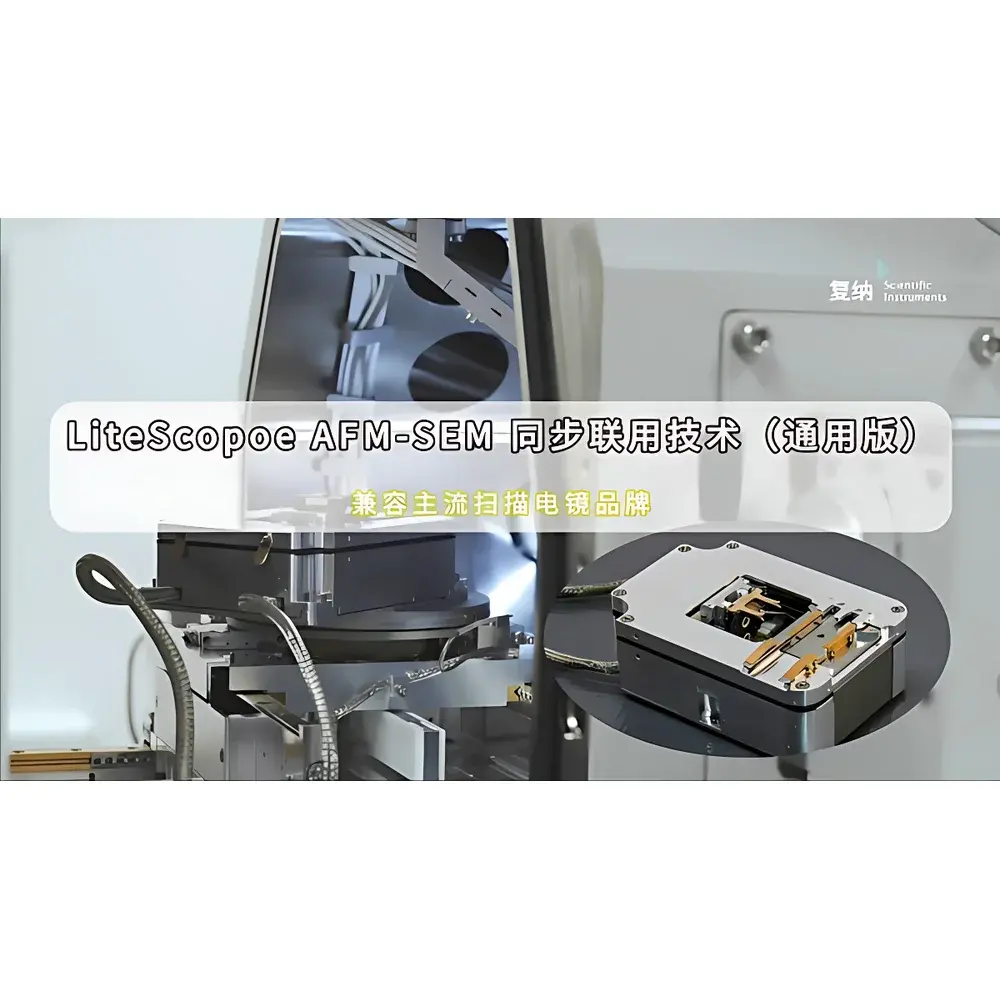
Phenom LiteScope AFM-SEM Correlative Microscopy System
| Brand | Phenom |
|---|---|
| Origin | Netherlands |
| Manufacturer Type | Authorized Distributor |
| Origin Category | Imported |
| Model | LiteScope |
| Instrument Type | Atomic Force Microscope |
| Sample Dimensions | 21 mm × 11 mm × 8 mm |
| Closed-Loop Scan Range | 80 µm × 80 µm × 16 µm |
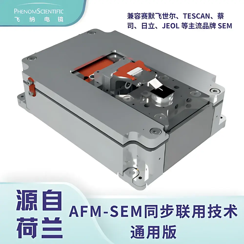
| Compatibility | Thermo Fisher, TESCAN, Zeiss, Hitachi, JEOL SEM platforms (custom integration available) |
| Measurement Modes | Contact/Non-contact AFM, Phase Imaging, Energy Dissipation Mapping, C-AFM, KPFM, EFM, STM, MFM, PFM, Force–Distance (F–z), Current–Voltage (I–V), CPEM Correlative Analysis |
Overview
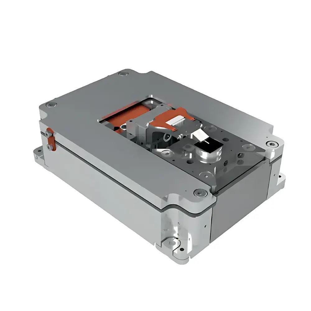
The Phenom LiteScope AFM-SEM Correlative Microscopy System is an engineered solution for in situ, spatially registered multimodal characterization at the nanoscale. It integrates a high-stability atomic force microscope directly within the chamber of a scanning electron microscope—enabling simultaneous acquisition of topographic, mechanical, electrical, magnetic, and electrochemical data from the exact same sample location, under identical vacuum or controlled-environment conditions. Unlike post-hoc correlation methods requiring sample relocation and re-imaging, the LiteScope implements true real-time co-localization: the AFM probe position is continuously tracked and overlaid onto live SEM images via calibrated coordinate mapping. This architecture is grounded in piezo-driven closed-loop positioning, electromagnetic interference (EMI)-shielded probe electronics, and vibration-damped mechanical coupling—ensuring sub-nanometer positional fidelity during concurrent SEM imaging and AFM scanning. The system is designed to operate across standard SEM working distances (WD ≥ 5 mm) and chamber configurations without compromising beam path integrity or detector efficiency.
Key Features
- In situ co-registered imaging: Simultaneous SEM and AFM data acquisition from identical coordinates, eliminating registration error inherent in sequential analysis.
- Real-time probe navigation: Live SEM video feed enables precise tip placement on sub-micron features—including suspended nanostructures, FIB-milled cross-sections, or electrode interfaces—without blind probing.
- Multi-parameter nanomechanical quantification: Closed-loop z-scanning supports quantitative force spectroscopy (F–z), elastic modulus mapping (via Hertz or Sneddon modeling), and nanohardness evaluation when paired with optional nanoindenter modules.
- Electrical and functional property mapping: Conductive-AFM (C-AFM), Kelvin Probe Force Microscopy (KPFM), Electrostatic Force Microscopy (EFM), Magnetic Force Microscopy (MFM), and Piezoresponse Force Microscopy (PFM) are implemented with low-noise current amplification (<1 pA resolution) and phase-locked loop (PLL) bias control.
- Modular expandability: Integrated sample rotation stage enables multi-sample analysis without venting; environmental chamber compatibility (NenoCase) allows ambient, inert-gas, or variable-humidity operation; optional digital camera navigation enhances coarse positioning accuracy outside SEM vacuum.
Sample Compatibility & Compliance
The LiteScope accommodates standard SEM stub-mounted samples up to 21 mm × 11 mm × 8 mm, including conductive and non-conductive substrates, battery electrodes, thin-film heterostructures, and biological cryo-sections. Its mechanical interface complies with ISO 2768-mK general tolerances and incorporates anti-backlash kinematic mounts compatible with Thermo Fisher’s Quanta, TESCAN’s MIRA, Zeiss’s Sigma series, Hitachi’s SU-series, and JEOL’s JSM-platforms. All electrical subsystems meet IEC 61000-4-3 EMC immunity standards. Data acquisition workflows support audit-trail generation per FDA 21 CFR Part 11 requirements when used in regulated environments (e.g., battery R&D under GLP protocols). Calibration artifacts traceable to NIST SRM 2100 and PTB reference standards are provided for lateral and vertical metrology validation.
Software & Data Management
Control and analysis are performed through Phenom’s CorrScope Suite—a modular application built on Qt/C++ with Python API access. The software synchronizes SEM frame timestamps with AFM scan lines and force curves, enabling pixel-to-pixel overlay of topography, secondary electron contrast, EDS elemental maps, and AFM-derived parameter channels (e.g., adhesion, dissipation, surface potential). Raw datasets are stored in HDF5 format with embedded metadata (scan parameters, calibration constants, instrument configuration), ensuring FAIR (Findable, Accessible, Interoperable, Reusable) compliance. Batch processing pipelines support automated feature segmentation, statistical roughness analysis (Sa, Sq, Sz per ISO 25178), and machine-learning-assisted phase classification (e.g., distinguishing ferrite/austenite domains in dual-phase steels using combined MFM + SEM + EDS inputs).
Applications
- Metallurgical microstructure-property correlation: Simultaneous SEM grain boundary identification, MFM magnetic domain imaging, and KPFM surface potential mapping on heat-treated steels reveal localized galvanic coupling mechanisms between phases.
- Next-generation battery interface science: In situ C-AFM conductivity mapping on cross-sectioned solid-state battery cathodes (e.g., NMC/Li₃PS₄ composites) quantifies interfacial charge transport barriers without air exposure—critical for mitigating parasitic side reactions.
- Nanomechanics of suspended architectures: Force-distance spectroscopy on spider silk nanowires or MEMS cantilevers, guided by real-time SEM visualization, yields Young’s modulus and fracture strain with <5% uncertainty—validated against tensile testing benchmarks.
- FIB-SEM-AFM tri-modal workflow: Site-specific lamella preparation followed by immediate AFM-based residual stress assessment on TEM lift-outs, enabled by the integrated rotation stage and vacuum-compatible probe exchange.
FAQ
Is the LiteScope compatible with field-emission SEMs (FE-SEMs)?
Yes—the system maintains compatibility with FE-SEMs operating at accelerating voltages from 1 kV to 30 kV, provided the working distance exceeds 5 mm and chamber port geometry permits mechanical integration.
Can KPFM measurements be performed under low-vacuum or ESEM conditions?
KPFM requires high vacuum (≤10⁻⁴ Pa) for stable electrostatic feedback; however, ambient-mode KPFM is supported via the NenoCase environmental module with active humidity control.
What level of spatial registration accuracy is achieved between SEM and AFM coordinate systems?
Typical registration uncertainty is ≤50 nm RMS after initial calibration using fiducial markers, verified via repeated cross-correlation of SEM and AFM topography on Si grating standards.
Does the system support automated region-of-interest (ROI) transfer from SEM to AFM?
Yes—users can define ROIs in SEM mode, and the software automatically calculates the corresponding AFM scan window, compensating for thermal drift and stage hysteresis in real time.
Are third-party AFM probes supported?
All standard commercial AFM probes with 125 µm × 125 µm × 20 µm chip dimensions and silicon nitride or conductive diamond tips are mechanically and electrically compatible.


