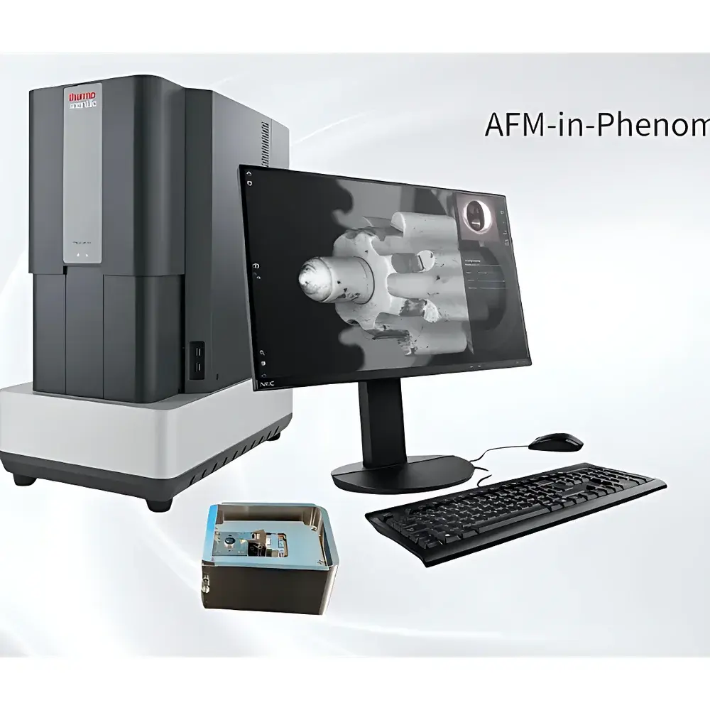
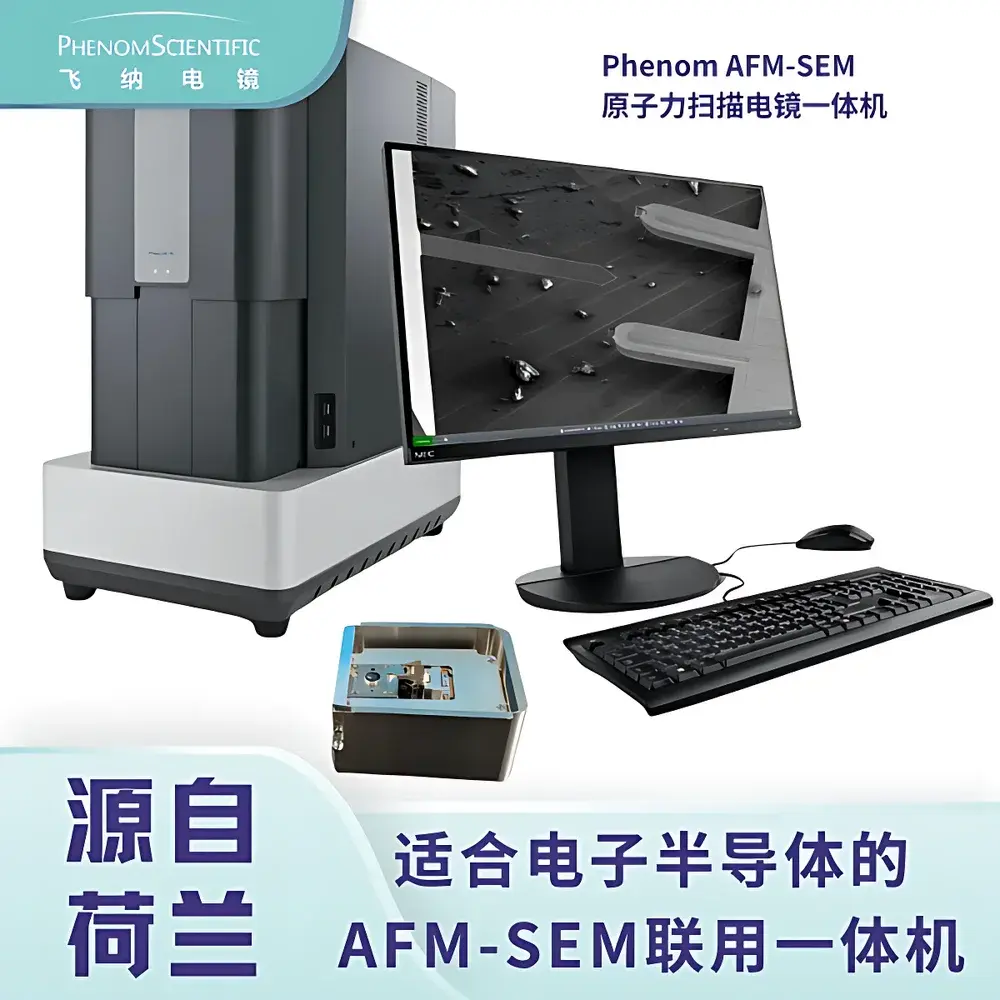
Phenom AFM-SEM Integrated Atomic Force and Scanning Electron Microscope
| Brand | Phenom |
|---|---|
| Origin | Netherlands |
| Model | AFM-in-Phenom XL |
| Instrument Type | Benchtop SEM-AFM Hybrid System |
| Electron Source | Cerium Hexaboride (CeB₆) |
| Maximum Sample Dimensions | 21 mm × 11 mm × 8 mm |
| Sample Weight Limit | 100 g |
| Open-Loop Scan Range | 100 µm × 100 µm × 20 µm |
| Closed-Loop Scan Range | 80 µm × 80 µm × 16 µm |
| Spatial Resolution (XY/Z) | 0.2 nm × 0.2 nm / 0.04 nm |
| Compatible Modes | Topography, Roughness, CAFM, KPFM, FMM, PFM, EFM, Force-Distance (F-z), Current-Voltage (I-V) |
Overview
The Phenom AFM-in-Phenom XL is a fully integrated benchtop hybrid system that co-localizes high-resolution scanning electron microscopy (SEM) and atomic force microscopy (AFM) within a single vacuum-compatible platform. Engineered for precision nanoscale characterization in semiconductor R&D, the system enables true multimodal correlative imaging—simultaneously acquiring structural, compositional, electrical, mechanical, and magnetic information from the same region of interest (ROI). Unlike conventional sequential or post-hoc correlation approaches, the AFM-in-Phenom XL maintains sample position stability at sub-nanometer levels across both modalities via shared coordinate referencing and real-time stage synchronization. The CeB₆ thermionic electron source delivers stable, high-brightness imaging at accelerating voltages from 5 kV to 15 kV, while the integrated AFM head employs low-noise piezoelectric scanners with closed-loop feedback control for quantitative nanomechanical and electrostatic measurements. This architecture eliminates registration errors inherent in separate-instrument workflows—critical when analyzing heterogeneous 2D materials, gate oxides, interfacial defects, or nanoscale dopant distributions in advanced logic and memory devices.
Key Features
- Benchtop footprint (≤ 0.5 m²) with integrated vacuum chamber (base pressure < 1×10⁻⁴ Pa), eliminating need for dedicated SEM labs or external vibration isolation.
- Simultaneous dual-beam operation: SEM imaging (secondary electron and backscattered electron detection) concurrent with AFM probe scanning—no repositioning or sample transfer required.
- Closed-loop XYZ piezo scanner with 80 µm × 80 µm × 16 µm range and < 0.04 nm Z-resolution, enabling quantitative nanomechanical mapping (modulus, adhesion, dissipation) and nanoelectrical profiling (surface potential, capacitance gradient, current leakage).
- Multi-functional AFM mode support: Conductive AFM (CAFM), Kelvin Probe Force Microscopy (KPFM), Magnetic Force Microscopy (MFM), Piezoresponse Force Microscopy (PFM), Electrostatic Force Microscopy (EFM), and force-distance/I-V spectroscopy—all calibrated and traceable to NIST-traceable standards.
- Automated alignment workflow: SEM-based navigation guides AFM probe positioning to sub-micron accuracy; integrated optical microscope (5×–50×) provides coarse-to-fine targeting.
Sample Compatibility & Compliance
The AFM-in-Phenom XL accommodates standard semiconductor wafer fragments, TEM lamellae, cross-sectioned devices, and 2D material flakes up to 21 mm × 11 mm × 8 mm and 100 g. Samples require no conductive coating for most SEM imaging due to low-kV operation and charge compensation capability. The system complies with IEC 61000-4-2 (ESD immunity), ISO 14644-1 Class 5 cleanroom compatibility (when operated in controlled environments), and supports GLP/GMP-aligned data integrity through audit-trail-enabled acquisition logs. All measurement parameters—including voltage ramps, scan speed, setpoint, and gain—are digitally recorded and exportable in HDF5 or TIFF+XML metadata format per ASTM E2793-21 guidelines for nanoscale imaging data reporting.
Software & Data Management
Control and analysis are unified under Phenom’s proprietary Phenom Desktop Software v5.x, featuring a modular, scriptable Python API (PyPhenom) for custom automation and integration into semiconductor process control systems. Raw datasets include synchronized timestamped SEM frames and AFM force volumes, with pixel-registered overlays generated automatically. Quantitative analysis modules support ISO 25178-compliant surface texture parameters (Sa, Sq, Sdr), current density mapping (nA/µm²), work function histograms (eV), and phase-resolved piezoelectric coefficient extraction (pm/V). Data exports meet FDA 21 CFR Part 11 requirements for electronic records and signatures when configured with user authentication, role-based access, and immutable audit trails.
Applications
This system is routinely deployed in university cleanrooms and industrial R&D labs for failure analysis of FinFETs and GAA transistors, metrology of ALD-grown high-k dielectrics, defect localization in EUV photoresists, and structure–property correlation in transition metal dichalcogenides (e.g., MoS₂, WSe₂). In published case studies, researchers used simultaneous SEM/EFM/phase imaging to distinguish monolayer vs. bilayer MoS₂ domains on SiO₂/Si substrates, correlate grain boundary conductivity (via CAFM) with local topography (AFM), and quantify contact potential difference shifts induced by thermal annealing—all within a single vacuum cycle. The platform also supports in situ electrical biasing (±10 V, 1 pA–100 µA range) and temperature-controlled stages (−20 °C to +80 °C) for dynamic property mapping.
FAQ
Is the AFM probe compatible with standard commercial cantilevers?
Yes—the system accepts industry-standard rectangular and triangular silicon/silicon nitride cantilevers (e.g., Bruker, Nanoworld, Olympus) with nominal spring constants from 0.01 N/m to 40 N/m.
Can the system perform automated defect review (ADR) across large fields of view?
While not a full-wafer inspection tool, the integrated navigation enables tile-based stitching of up to 100 SEM+AFM fields (each ≤ 80 µm²) with automated feature detection and ROI prioritization using machine-learning-assisted pattern recognition.
Does the software support batch processing of I-V curves across multiple locations?
Yes—customizable scripting allows automated acquisition and statistical fitting (e.g., Schottky barrier height, trap density) across >1,000 spatially resolved I-V spectra per session.
What vacuum level is required for AFM operation?
AFM scanning occurs at the same base pressure as SEM imaging (< 1×10⁻⁴ Pa); no additional pumping or differential pumping stages are needed.
How is calibration traceability maintained for quantitative AFM measurements?
All lateral and vertical calibrations are performed using NIST-traceable grating standards (Pitch: 210 nm, Step Height: 20 nm) and verified per ISO/IEC 17025-accredited procedures documented in the system’s Certificate of Calibration.