SPS030 Surface Photovoltage Spectroscopy System
| Origin | UK |
|---|---|
| Manufacturer Type | Authorized Distributor |
| Origin Category | Imported |
| Model | SPS030 |
| Price Range | USD 48,000 – 69,000 |
| Optical Configuration | Single-beam |
| Detector | Photomultiplier Tube (PMT) |
| Wavelength Range | 400–1000 nm |
| Wavelength Scanning | Motorized Automatic |
| Spectral Bandwidth | 25 nm (FWHM @ 400–700 nm), 45 nm (FWHM @ 400–1000 nm) |
| Wavelength Accuracy | ±2.0 nm |
| Stray Light | ≤0.01% |
Overview
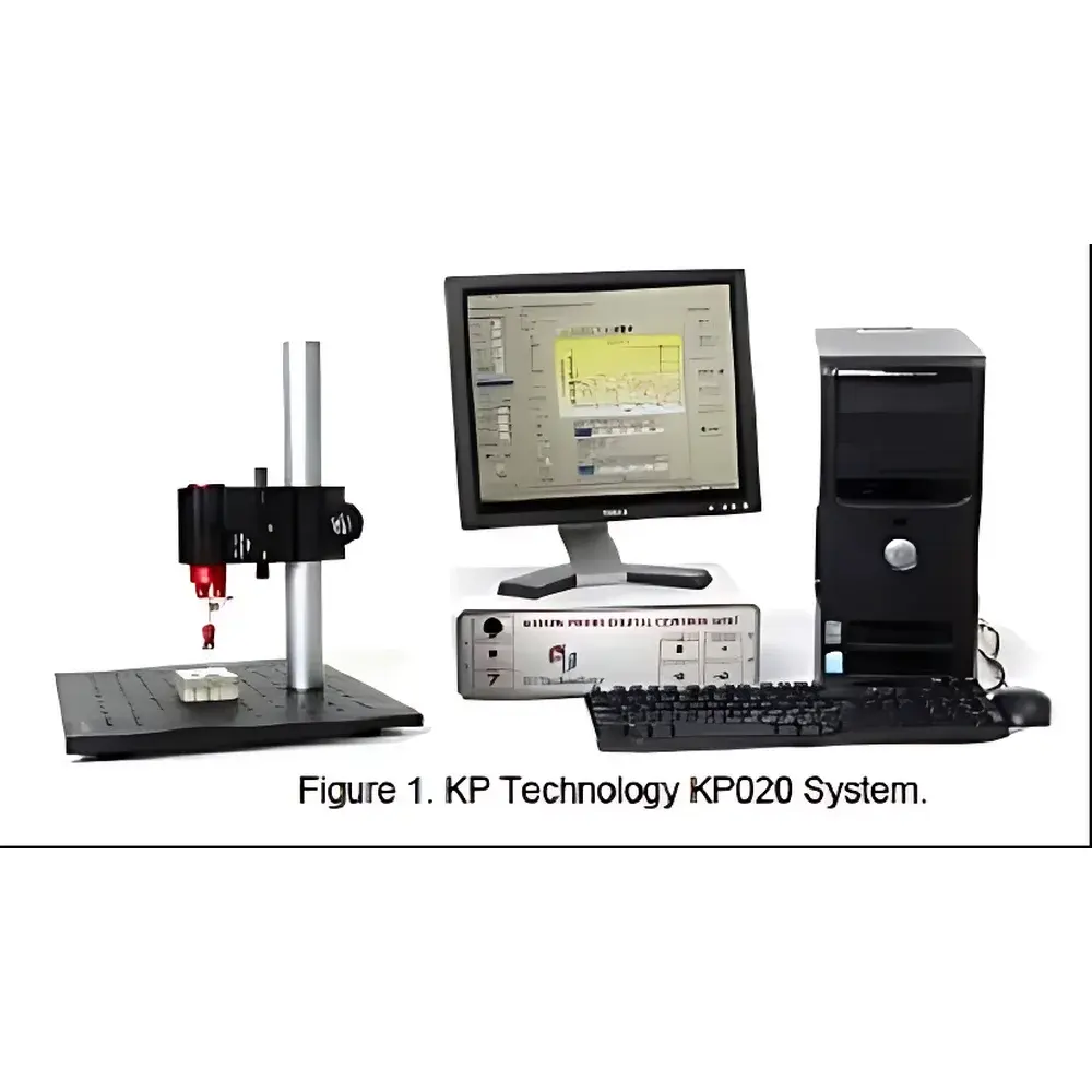
The SPS030 Surface Photovoltage Spectroscopy System is a purpose-engineered instrumentation platform for quantitative, non-contact characterization of photoinduced surface potential changes in semiconducting and photoactive materials. Operating on the principle of surface photovoltage (SPV) detection—where incident photons generate electron-hole pairs near the surface or depletion region, inducing measurable shifts in local work function—the SPS030 enables direct correlation between spectral excitation and charge separation dynamics. Unlike conventional UV-Vis absorbance measurements, SPV spectroscopy is highly sensitive to electronic defects, trap states, band bending, and interfacial recombination kinetics. The system integrates a stabilized 150 W DC quartz-tungsten-halogen (QTH) light source with fiber-coupled delivery, motorized monochromator, digital optical chopper, and high-gain PMT-based detection, all synchronized under unified software control. Designed for laboratory-scale R&D in photovoltaics, thin-film electronics, and functional material science, the SPS030 delivers reproducible, bias-free surface potential response across the visible to near-infrared spectrum (400–1000 nm).
Key Features
- Motorized monochromator with automatic wavelength scanning (400–1000 nm) and selectable spectral bandwidths: 25 nm FWHM (400–700 nm) and 45 nm FWHM (400–1000 nm)
- High-stability 150 W DC QTH lamp with integrated fiber-optic illumination path, enabling flexible top- or bottom-side sample illumination
- Digital intensity control (0–100%) with real-time feedback, ensuring precise photon flux calibration for quantitative SPV amplitude analysis
- Integrated lock-in compatible optical chopper (40–1200 Hz) for AC-mode SPV detection, supporting transient decay profiling and phase-resolved measurements
- Single-beam architecture with PMT detector optimized for low-noise, high-dynamic-range voltage signal acquisition (sub-mV resolution)
- Wavelength accuracy of ±2.0 nm and stray light level ≤0.01%, meeting ISO 9001-compliant optical performance benchmarks for analytical spectroscopy
Sample Compatibility & Compliance
The SPS030 accommodates planar solid-state samples up to 200 mm in diameter—including silicon wafers, perovskite thin films, organic photovoltaic layers, dye-sensitized electrodes, and III–V semiconductor heterostructures—using a modular, adjustable sample stage with vacuum-compatible mounting options. Sample positioning is facilitated by XYZ micrometer translation and tilt adjustment, ensuring optimal alignment with the fiber-coupled illumination spot. The system supports both ambient and inert-gas purged environments (N₂ or Ar) to minimize surface oxidation during measurement. All firmware and data acquisition protocols comply with GLP documentation standards; raw SPV spectra and metadata are timestamped and exportable in ASCII/CSV format for traceability. While not FDA 21 CFR Part 11 certified out-of-the-box, the software architecture supports audit trail configuration and user access controls upon site-specific validation.
Software & Data Management
The SPS S software suite provides full instrument orchestration via USB 2.0 interface, including monochromator positioning, chopper frequency/duty cycle, intensity ramping, and PMT gain optimization. Real-time plotting displays both DC SPV (steady-state surface potential shift) and AC SPV (amplitude/phase vs. wavelength), with built-in baseline correction, smoothing filters, and derivative analysis. Data sets are stored with embedded metadata (wavelength, intensity, integration time, chopper settings, ambient temperature/humidity). Export options include PNG/SVG graphics and tabular formats compatible with OriginLab, MATLAB, and Python (NumPy/Pandas). Batch processing scripts enable automated spectral series acquisition across multiple samples or bias conditions. Software updates are delivered via secure HTTPS portal with version-controlled release notes.
Applications
- Quantitative defect density mapping in crystalline and polycrystalline silicon wafers for solar cell process monitoring
- Band alignment and interface state analysis at heterojunctions in perovskite–metal oxide and organic–inorganic hybrid devices
- Photocharge separation efficiency assessment in photocatalytic materials (e.g., TiO₂, g-C₃N₄, BiVO₄)
- Time-resolved SPV decay kinetics for carrier lifetime estimation under modulated illumination
- Correlation of SPV onset edge with optical bandgap and Urbach energy in amorphous semiconductors
- Screening of surface passivation quality in SiNx-coated c-Si substrates using sub-bandgap excitation
FAQ
What types of samples can be measured with the SPS030?
Solid, non-powdered, electrically insulating or semiconducting planar samples—such as wafers, coated glass substrates, or spin-cast thin films—with minimum lateral dimensions of 5 mm × 5 mm and thickness ≥10 µm.
Is electrical contact required for SPV measurement?
No. Surface photovoltage spectroscopy is a non-contact, capacitively coupled technique; no electrode deposition or wiring is needed.
Can the system operate under controlled atmosphere?
Yes. The sample chamber accommodates optional glovebox integration or purge gas inlet ports for O₂/H₂O-sensitive measurements.
How is wavelength calibration verified?
Factory calibration uses NIST-traceable mercury–argon emission lines; users may perform periodic verification using optional Hg/Ar lamp accessory.
Does the system support external biasing or Kelvin probe integration?
The SPS030 is fully compatible with third-party Kelvin probe force microscopy (KPFM) controllers and external voltage bias units via analog I/O ports and TTL synchronization triggers.