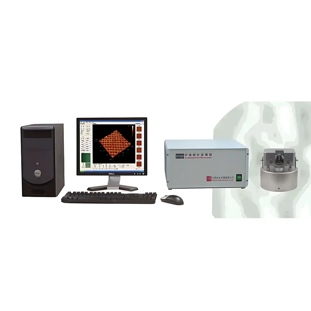
Benyuan Nano BY1000 Scanning Tunneling Microscope
| Brand | Benyuan Nano |
|---|---|
| Origin | Beijing, China |
| Manufacturer Type | Authorized Distributor |
| Product Origin | Domestic (China) |
| Model | BY1000 |
| Price Range | USD 14,000 – 70,000 |
| Instrument Type | Scanning Tunneling Microscope (STM) |
| Position Detection Noise | 0.1 Å RMS |
| Maximum Sample Size | Ø45 mm × 15 mm |
| XY Sample Stage Travel Range | 100 mm × 100 mm |
Overview
The Benyuan Nano BY1000 Scanning Tunneling Microscope (STM) is a high-stability, ultra-high-resolution surface characterization instrument engineered for atomic-scale imaging and spectroscopic analysis under ambient or controlled environmental conditions. Based on quantum mechanical tunneling current detection between a conductive tip and a conductive sample surface, the BY1000 delivers sub-angstrom vertical resolution (≤0.01 nm) and lateral resolution of ≤0.1 nm—enabling direct visualization of atomic lattices, surface reconstructions, adsorbate arrangements, and electronic density variations. Its robust mechanical architecture integrates low-drift piezoelectric scanners with active vibration isolation compatibility, while the large-sample chamber design accommodates specimens up to Ø45 mm in diameter and 15 mm in thickness—supporting diverse materials including single crystals, thin films, 2D materials (e.g., graphene, TMDCs), and nanostructured electrodes without requiring extensive sample preparation or sectioning.
Key Features
- Integrated multimodal scanning probe platform supporting STM, Atomic Force Microscopy (AFM), and Lateral Force Microscopy (LFM) via interchangeable probe holders—no hardware reconfiguration required.
- Dedicated real-time control system built around a Texas Instruments (TI) 32-bit digital signal processor (DSP), ensuring deterministic loop timing and sub-millisecond feedback response.
- Five-channel Apex high-voltage operational amplifier stack for precise, low-noise Z-scanner actuation with <0.1 Å RMS position detection noise.
- Fully automated tip approach sequence—eliminating manual coarse positioning—and enabling reproducible tip–sample junction formation across multiple users and sessions.
- Dual-mode data acquisition: simultaneous multi-channel signal capture (topography, tunneling current, I–V, I–Z, force–distance) during a single scan pass.
- Fast Ethernet (10/100 Mbps) interface for low-latency communication with host PC; compatible with Windows 2000/XP-based acquisition and processing software.
- On-the-fly 3D surface rendering with adjustable perspective, lighting, and false-color mapping; supports real-time cross-sectional profiling and height histogram generation.
Sample Compatibility & Compliance
The BY1000 accommodates electrically conductive or semi-conductive samples—including metals, doped semiconductors, graphite, epitaxial thin films, and electrochemically deposited layers. Non-conductive substrates may be analyzed using conductive coatings (e.g., Au/Pd sputtering) or in AFM mode. The 100 mm × 100 mm motorized XY stage allows precise navigation over large-area samples, while the 15 mm vertical travel range supports thick or topographically complex specimens. All firmware and software modules are designed to support GLP-compliant workflows: audit trails for parameter changes, timestamped image metadata, and full raw-data export (binary + ASCII formats) ensure traceability for ISO/IEC 17025-accredited laboratories. Though not FDA-certified as a medical device, the system meets general laboratory instrumentation requirements per IEC 61010-1 for electrical safety and electromagnetic compatibility.
Software & Data Management
The native Windows-based control suite provides integrated instrument setup, real-time scanning, offline analysis, and reporting functions. It includes automated roughness quantification per ISO 25178 and ASME B46.1 standards (Sa, Sq, Sz, Sdr, etc.), particle analysis (size, distribution, aspect ratio), and tip characterization algorithms (tip convolution modeling, blind reconstruction, and tip–sample deconvolution). All acquired images and spectroscopic curves retain full 16-bit depth and are stored with embedded calibration parameters (scan size, setpoint, gain, filter settings). Export options include TIFF, BMP, PNG, CSV, and proprietary .BYS binary format—ensuring compatibility with third-party tools such as Gwyddion, ImageJ/Fiji, MATLAB, and Python-based analysis pipelines. Software updates and remote diagnostics are supported via secure HTTPS channels.
Applications
The BY1000 serves advanced research and quality control applications across nanomaterials science, surface physics, electrochemistry, and microelectronics. Typical use cases include atomic-resolution imaging of Si(111)-7×7 reconstructions; in-situ monitoring of electrode processes in liquid cells; defect identification in CVD-grown MoS₂ monolayers; quantitative assessment of thin-film uniformity in OLED fabrication; and nanoscale conductivity mapping of doped polymer blends. Its dual STM/AFM capability enables correlative studies—for example, comparing local electronic states (via dI/dV mapping) with mechanical modulus (via force modulation)—without transferring samples between instruments.
FAQ
What is the maximum sample thickness supported by the BY1000?
The system accepts samples up to 15 mm in thickness, provided they fit within the Ø45 mm diameter constraint and remain mechanically stable during scanning.
Does the BY1000 support vacuum or cryogenic operation?
The standard configuration operates under ambient conditions. Vacuum and low-temperature variants are available as custom-engineered options upon request.
Can raw tunneling current data be exported for external spectral analysis?
Yes—full time-series current traces, I–V sweeps, and I–Z curves are saved in ASCII-compatible format with calibrated units and timestamps.
Is the software compliant with 21 CFR Part 11 requirements?
While the core acquisition software does not include electronic signature or role-based access controls out-of-the-box, it supports integration with validated LIMS or ELN systems that provide Part 11 compliance layers.
What probe types are compatible with the BY1000’s quick-swap holder?
Standard tungsten wire tips, Pt/Ir etched probes, and commercial silicon AFM cantilevers (with integrated reflective coating) are supported; custom probe geometries can be accommodated via mechanical adapter kits.