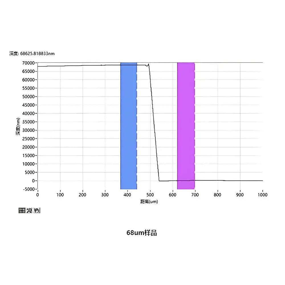
ZEPTOOLS JS10B Manual Stylus Profilometer
| Brand | ZEPTOOLS |
|---|---|
| Model | JS10B |
| Origin | Anhui, China |
| Measurement Range | 80 µm |
| Probe Normal Force | 0.5–50 mg |
| Step Height Repeatability | ≤0.5 nm (1σ, 30 scans on 1 µm Si standard) |
| Vertical Resolution | 0.05 nm (full scale) |
| Maximum Sample Size | ≤150 mm |
| Probe Tip Radius | ≥2 µm (standard, 60° included angle) |
| Optional Probe | ≤1 µm radius, 60° |
| Scan Speed | 5–100 µm/s |
| Sampling Rate | 200 Hz |
| Max Data Points per Scan | 2×10⁶ |
| XY Stage Travel | 150 mm (manual coarse/fine adjustment) |
| Z-Stage Travel | 10 mm |
| Rotary Stage | ±360° |
| Sample Thickness Limit | ≤10 mm |
| Compatible Substrates | Si, LiTaO₃, glass (opaque or semi-transparent) |
Overview
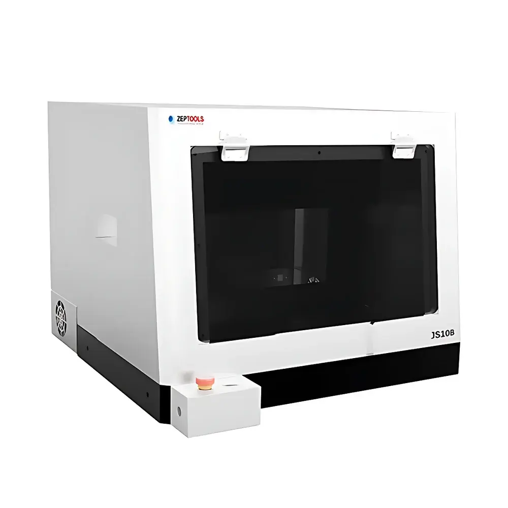
The ZEPTOOLS JS10B Manual Stylus Profilometer is a precision contact-based surface metrology instrument engineered for nanoscale step height, film thickness, surface topography, waviness, and roughness characterization. It operates on the principle of mechanical stylus profiling—where a diamond-tipped probe physically traverses the sample surface in controlled lateral motion, transducing vertical displacement into high-fidelity analog signals via a high-stability differential inductive sensor. The system employs closed-loop force regulation to maintain constant normal load during scanning, minimizing ploughing artifacts on soft or compliant films while preserving measurement fidelity on hard substrates such as silicon wafers and optical glass. Designed for laboratory environments where cost-effectiveness, operational simplicity, and traceable nanometrology are critical, the JS10B delivers sub-nanometer repeatability without requiring active vibration isolation under typical benchtop conditions. Its architecture conforms to foundational principles outlined in ISO 25178-2 (areal surface texture) and ISO 4287 (profile-based roughness), supporting compliance-driven workflows in academic research, semiconductor process development, and microfabrication QA/QC.
Key Features
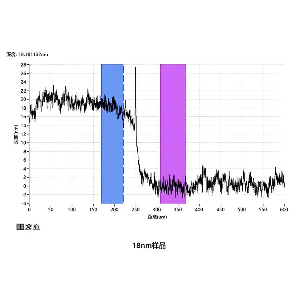
- Sub-nanometer vertical resolution (0.05 nm full-scale) with verified ≤0.5 nm (1σ) repeatability on certified 1 µm step standards—validated across 30 consecutive scans.
- Adjustable probe normal force (0.5–50 mg) via calibrated micro-spring mechanism, enabling optimization for fragile polymer films, photoresists, or brittle oxide layers without tip wear or surface deformation.
- Integrated coaxial optical viewing system with real-time video feed, allowing precise alignment of probe tip to target features (e.g., etch stops, mask edges, MEMS release structures) prior to scanning.
- Manually actuated XYZR stage with 150 mm XY travel (dual-range coarse/fine control), 10 mm Z lift, and full ±360° rotation—supporting angular profiling and multi-directional cross-section analysis.
- High-density data acquisition at up to 200 Hz sampling rate and 2 million points per scan, ensuring robust statistical representation of surface heterogeneity over extended profiles.
- Compact footprint (<600 × 450 × 300 mm) and tool-free probe exchange design facilitate integration into cleanroom workbenches and shared instrumentation facilities.
Sample Compatibility & Compliance
The JS10B accommodates rigid and semi-rigid planar substrates up to 150 mm in diameter and 10 mm in thickness, including single-crystal silicon, lithium tantalate (LiTaO₃), fused silica, borosilicate glass, and sapphire. It is not intended for highly elastic, viscoelastic, or ultra-low-modulus materials (e.g., hydrogels, uncured polymers) due to inherent contact mechanics constraints. All measurements adhere to ASTM E1555–22 (Standard Practice for Measurement of Surface Roughness Using Contact Profilometers) and support traceability through NIST-traceable step height calibration artifacts (optional). While the instrument itself does not enforce electronic audit trails, its raw profile data (.txt/.csv) and metadata export structure enable post-acquisition alignment with GLP and GMP documentation requirements when integrated into validated lab information management systems (LIMS).
Software & Data Management
The bundled ZEPTOOLS Profilometry Suite provides intuitive GUI-based control for scan setup, real-time preview, and post-processing. Core modules include step height quantification (ISO 5436-1 compliant), roughness parameter calculation (Ra, Rq, Rz, Rsk, Rku), waviness filtering (Gaussian or spline), and thin-film stress estimation via substrate curvature analysis (Stoney equation implementation). Data files store timestamped acquisition parameters, environmental notes, and user-defined annotations—facilitating retrospective review and regulatory reporting. Export options include CSV, BMP, TIFF, and XML formats compatible with third-party analysis platforms (e.g., MountainsMap®, MATLAB, Python SciPy). Software supports multi-language UI (English default) and runs on Windows 10/11 (64-bit) with minimum i5 CPU, 8 GB RAM, and dedicated GPU recommended for real-time rendering of large datasets.
Applications
- Quantitative thickness metrology of deposited layers (e.g., PECVD SiNx, ALD Al2O3, sputtered ITO) and etched features in CMOS, MEMS, and compound semiconductor fabrication.
- Roughness and waviness assessment of polished wafers, optical coatings, and medical device surfaces per ISO 13565 and USP .
- Residual stress evaluation of thin films via curvature-induced step height asymmetry on patterned cantilevers or blanket test wafers.
- Process validation for lithography, lift-off, and reactive ion etching—particularly where cross-sectional SEM is impractical or destructive.
- Teaching and method development in university labs focused on surface science, materials engineering, and nanofabrication technology transfer.
FAQ
What types of probes are supported, and how do they affect measurement fidelity?
The JS10B ships with a standard 2 µm radius, 60° included-angle diamond probe optimized for general-purpose profiling. Optional sub-micron tips (≤1 µm radius) are available for high-resolution edge definition on steep sidewalls or narrow trenches, though they require stricter force control and more frequent inspection for wear.
Is the system compatible with automated stage integration or external trigger inputs?
No—the JS10B is strictly manual-stage operated and lacks TTL or USB-CI interfaces for external synchronization. Automation-ready variants (e.g., JS200 series) are offered separately.
Can the software generate reports compliant with ISO/IEC 17025 or FDA 21 CFR Part 11?
The base software does not implement electronic signatures, audit trails, or role-based access control. However, exported data files and metadata logs can be ingested into validated LIMS or ELN platforms that meet those regulatory requirements.
What environmental conditions are recommended for optimal performance?
Operation is specified for ambient temperatures of 20–25 °C ±1 °C, humidity 10 Hz). A passive granite slab is sufficient; active isolation is unnecessary unless measuring below 0.2 nm RMS noise floor.
How is probe calibration performed, and what maintenance is required?
Probe geometry is verified using certified step-height standards (e.g., 1 µm Si reference). Daily visual inspection under optical magnification and weekly cleaning with isopropyl alcohol and lint-free swabs are recommended. Full recalibration of the vertical sensor is advised annually or after mechanical shock.