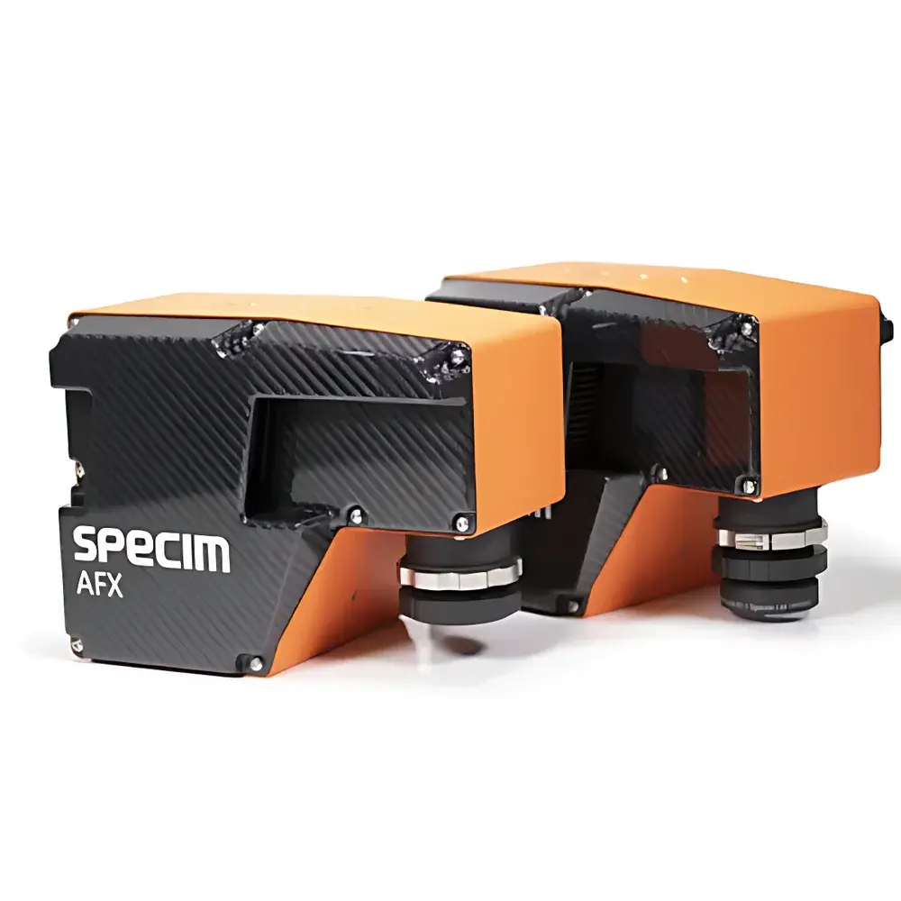
Nanobase AUT-XperP-Projector Maskless Smart Projection Photocurrent System
| Brand | Nanobase |
|---|---|
| Origin | South Korea |
| Type | Confocal Micro-Raman Spectrometer with Integrated Maskless Spatial Light Modulation |
| Excitation Architecture | DMD + SLM Dual-Modulated Wideband Illumination Platform |
| Optical Configuration | Upright Research-Grade Microscope Coupled to Broadband Source & Tunable Monochromatic Selection (VIS–NIR–MIR) |
| Software Integration | NanoSpectrum Suite with Keithley 2400/2600 Series SMU Compatibility |
| Compliance | GLP/GMP-ready data logging, ASTM E2587-compliant measurement traceability, ISO/IEC 17025-aligned calibration framework |
| Environmental Operation | Compatible with cryogenic stages (4 K–300 K), in-plane/out-of-plane magnetic fields (up to 9 T), and controlled-atmosphere chambers |
Overview
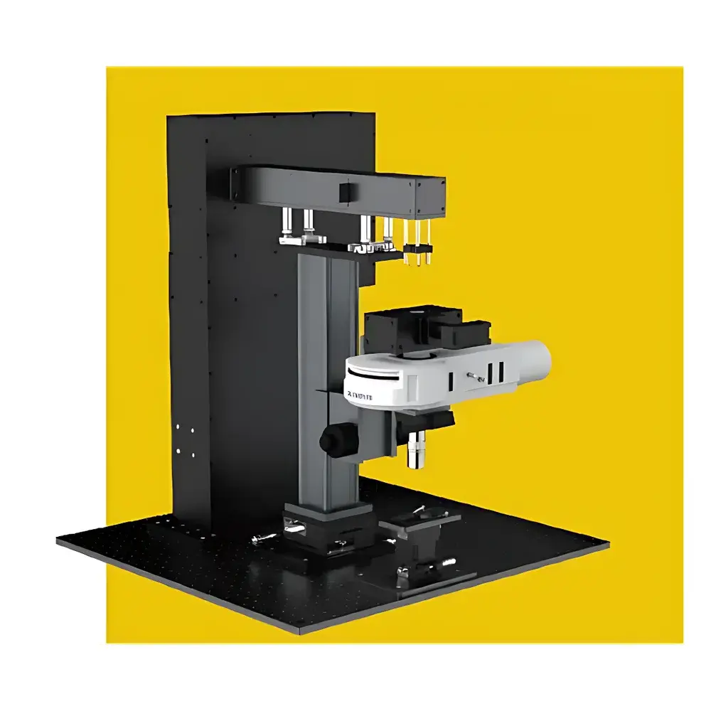
The Nanobase AUT-XperP-Projector is a purpose-built maskless smart projection photocurrent characterization system engineered for high-fidelity, spatially resolved optoelectronic interrogation of microscale and nanoscale arrayed devices. Unlike conventional point-scanning Raman or photocurrent platforms—whose sequential excitation fails to replicate real-world operational conditions—the AUT-XperP-Projector implements simultaneous, programmable illumination across the entire device array using a dual-modulation optical architecture. At its core lies a hybrid modulation engine combining a Digital Micromirror Device (DMD) for high-speed grayscale intensity and duty-cycle control (up to 22.3 kHz at 1-bit depth) and a Liquid-Crystal-based Spatial Light Modulator (SLM) for pixel-level wavefront phase and polarization state manipulation. This enables true spatiotemporal photostimulation: users project user-defined grayscale images, grayscale animations, or arbitrary polarization vector fields directly onto the sample plane—mimicking realistic illumination profiles encountered in imaging sensors, photovoltaic arrays, neuromorphic photodetectors, and metasurface-integrated optoelectronics. While classified under spectroscopy instrumentation due to its seamless integration with confocal Raman microscopy modules, the AUT-XperP-Projector operates fundamentally as a calibrated, metrology-grade photocurrent stimulus platform—not a passive spectral analyzer. Its optical path is optimized for quantitative photocurrent yield mapping, carrier dynamics probing, and polarization-resolved quantum efficiency assessment under physiologically relevant illumination conditions.
Key Features
- Dual independent modulation architecture: DMD for high-bandwidth grayscale/intensity control (0–100% duty cycle, 22.3 kHz @ 1-bit) and SLM for spatial phase/polarization synthesis (λ/6 wavefront fidelity @ 635 nm, 14.5 ms response)
- Wideband excitation compatibility: Integrated broadband white-light laser source (400–2400 nm) coupled with acousto-optic tunable filter (AOTF) or motorized monochromator for discrete wavelength selection across VIS, NIR, and MIR bands
- Multi-wavelength power normalization: Active feedback stabilization ensures identical irradiance (W/cm²) across all selected excitation wavelengths—critical for cross-spectral quantum efficiency comparison
- Real-time image-guided correction: On-the-fly projection alignment via integrated CMOS camera; software-driven closed-loop adjustment of intensity distribution based on back-reflected or fluorescence feedback
- Full environmental integration: Designed for operation inside cryostats (4 K–300 K), superconducting magnet bores (in-plane and out-of-plane field orientation), and gas-controlled gloveboxes (N₂, Ar, O₂, vacuum)
- Hardware-agnostic SMU interface: Native support for Keithley 2400/2600 Series Source Measure Units with full bidirectional command protocol (TSP-Link); extensible to other SMUs via custom SCPI scripting layer
Sample Compatibility & Compliance
The AUT-XperP-Projector accommodates standard probe station footprints (e.g., MS Tech, Semishare) and supports wafer-scale substrates up to 6-inch diameter. Its upright microscope configuration integrates flat-field semi-apochromatic objectives (10×–100×, long working distance options available) and motorized XYZ translation stages with sub-micron repeatability. All optical components meet ISO 10110 surface quality standards; laser safety complies with IEC 60825-1:2014 Class 3R/4 configurations depending on output configuration. Data acquisition adheres to ASTM E2587-22 guidelines for statistical process control in optoelectronic testing, and audit trails—including instrument parameters, projection masks, SMU settings, and environmental metadata—are recorded in timestamped, immutable logs compliant with FDA 21 CFR Part 11 requirements when operated under validated NanoSpectrum software protocols.
Software & Data Management
The NanoSpectrum software suite provides unified control of DMD/SLM modulation patterns, light source selection, environmental chamber parameters, and SMU synchronization. Users define stimulation sequences via intuitive drag-and-drop graphical interface or Python API (PyNanobase SDK). Projection masks are generated from bitmap inputs or algorithmically synthesized (e.g., radial polarization vortices, Hadamard-coded patterns, or custom Jones matrix maps). All raw photocurrent transients, spatial maps, and metadata are exported in standardized formats: SPM (Scanning Probe Microscopy) for interoperability with WSxM or Gwyddion, CSV for MATLAB/Python analysis, and HDF5 for large-scale dataset archiving. Built-in batch processing enables automated parameter sweeps (wavelength, polarization angle, intensity gradient) with pass/fail thresholds defined per device pixel.
Applications
- Quantitative performance mapping of CMOS image sensor arrays under realistic scene illumination (including motion blur emulation via grayscale animation projection)
- Polarization-sensitive characterization of chiral photodetectors, plasmonic metasurfaces, and 2D material heterostructures
- Carrier lifetime extraction via time-resolved photocurrent decay under spatially structured pulsed excitation
- Defect localization in perovskite solar cell arrays using localized grayscale gradient stress testing
- Neuromorphic photodetector validation under spatiotemporally coded stimuli mimicking retinal ganglion cell receptive fields
- Calibration-free quantum efficiency uniformity assessment across multi-junction photovoltaic tiles
FAQ
Does the AUT-XperP-Projector require external lasers for Raman spectroscopy?
No—it integrates a broadband white-light laser source suitable for both wideband photocurrent stimulation and optional Raman excitation when combined with spectrometer coupling. Discrete-wavelength lasers (e.g., 532 nm, 785 nm) may be added via fiber-coupled ports for enhanced Raman signal-to-noise.
Can the system perform time-resolved photocurrent measurements?
Yes—when synchronized with a pulsed light source (internal or external) and a fast digitizer (e.g., Keysight M3202A), it achieves sub-nanosecond temporal resolution for transient photocurrent analysis.
Is the NanoSpectrum software validated for regulated environments?
The software includes optional IQ/OQ documentation packages and supports 21 CFR Part 11 electronic signature workflows when deployed on validated Windows OS configurations.
What is the maximum usable numerical aperture for objective coupling?
The optical train supports NA up to 0.95 with oil-immersion objectives; maximum working distance is 34 mm for dry long-working-distance lenses.
How is polarization uniformity calibrated across the projection field?
Factory calibration uses a Mueller matrix imaging polarimeter; residual spatial non-uniformity (< ±1.2° retardance error) is corrected via real-time algorithmic compensation during SLM addressing.