SURAGUS EddyCus TF Inline Sheet Resistance Monitor (Eddy Current-Based Non-Contact Metrology System)
| Brand | SURAGUS |
|---|---|
| Origin | Germany |
| Manufacturer Type | OEM Instrument Manufacturer |
| Measurement Principle | Eddy Current Sensing |
| Sampling Rate | Up to 1000 Hz |
| Sheet Resistance Range | 0.1 mΩ/□ to 1 kΩ/□ |
| Metal Layer Thickness Range | 2 nm – 2 mm (material-dependent) |
| Resistivity Range | 0.1 mΩ·cm – 1 Ω·cm |
| Distance-to-Target Gap | Up to 60 mm |
| Compliance | CE, RoHS, ISO 9001-certified design |
| Environmental Operation | Ambient atmosphere or vacuum-compatible |
Overview
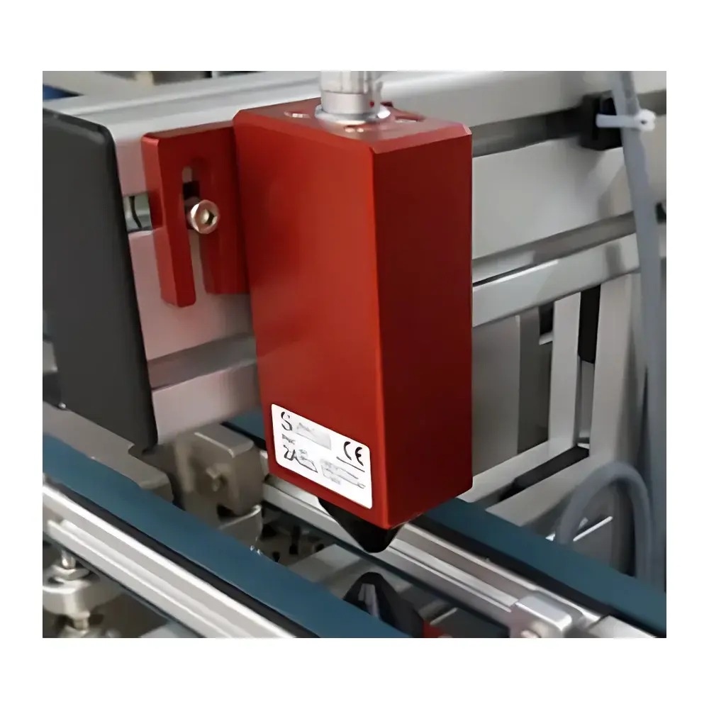
The SURAGUS EddyCus TF Inline Sheet Resistance Monitor is a high-speed, non-contact eddy current metrology system engineered for real-time characterization of conductive thin films during continuous industrial manufacturing. Operating on the principle of electromagnetic induction, it measures the perturbation of a high-frequency alternating magnetic field generated by a probe coil interacting with conductive layers—enabling precise determination of sheet resistance (Rs), metal thickness, resistivity, and related functional properties without physical contact or process interruption. Designed for integration into roll-to-roll (R2R), wafer processing, web coating, and vacuum deposition lines, the system supports in-situ monitoring of PVD (sputtering, evaporation), CVD, electroplating, slot-die coating, spray deposition, inkjet printing, and thermal annealing/sintering processes. Its robust architecture ensures stable performance under dynamic thermal and mechanical conditions typical of high-throughput production environments.
Key Features
- Non-contact measurement with standoff distance up to 60 mm—eliminating risk of substrate damage or contamination
- High temporal resolution: up to 1000 measurements per second for capturing transient film evolution during fast-moving web or rotating wafer processes
- Multi-channel scalability: configurable from 1 to 99 independent sensor channels per system for spatially resolved mapping across wide substrates
- Temperature-compensated electronics enabling long-term measurement stability in ambient or thermally fluctuating environments
- Modular probe mounting options: fixed-point installation or traversing carriage integration for edge-near or full-width profiling
- Vacuum-rated variants available for integration into UHV sputter chambers or MBE systems
- Material-agnostic calibration framework supporting metals (Cu, Al, Ag, ITO), doped semiconductors, conductive polymers, and transparent conductive oxides
Sample Compatibility & Compliance
The EddyCus TF system accommodates a broad range of substrate materials—including silicon wafers, glass, PET/PEN foils, paper, ceramic tiles, and flexible polymer films—regardless of optical transparency or surface roughness. It delivers traceable measurements compliant with international standards governing thin-film electrical metrology, including ASTM F84 (Standard Test Method for Measuring Resistivity of Silicon Wafers), ISO 10474 (Metallic products — Types of inspection documents), and SEMI MF1530 (Guide for Sheet Resistance Measurements). All firmware and data handling modules are designed to support GLP/GMP-aligned audit trails, and optional 21 CFR Part 11-compliant software packages are available for regulated pharmaceutical or medical device manufacturing environments.
Software & Data Management
The system interfaces natively with factory automation infrastructures via EtherCAT, PROFINET, or Modbus TCP protocols, enabling direct feed of Rs values into MES, SCADA, or APC platforms. SURAGUS provides two complementary software suites: EddyCus EC Control—a standalone Windows application for real-time visualization, trend logging, statistical process control (SPC) charting, and offline spectral analysis—and an open API (C++, .NET, Python) for custom integration into proprietary process control logic. All raw time-series data are stored in HDF5 format with embedded metadata (timestamp, sensor ID, temperature, gap distance), ensuring FAIR (Findable, Accessible, Interoperable, Reusable) data management principles.
Applications
This instrument serves critical quality assurance functions across multiple advanced manufacturing domains: monitoring uniformity of ITO or AZO layers in display fabrication; tracking copper seed layer integrity pre-electrofill in semiconductor interconnect processes; verifying silver nanoparticle ink sintering kinetics in printed electronics; quantifying residual moisture content in barrier-coated flexible packaging via dielectric permittivity correlation; assessing doping homogeneity in solar cell emitter formation; and evaluating post-etch conductivity recovery in MEMS release processes. It is also deployed in R&D settings for rapid screening of novel conductive nanocomposites and self-assembled monolayers.
FAQ
What physical property does the EddyCus TF system measure directly?
It directly measures the eddy current damping effect induced in conductive thin films, from which sheet resistance (Rs) is derived using calibrated transfer functions.
Can the system distinguish between changes in thickness and changes in conductivity?
Yes—when combined with multi-frequency excitation or reference material calibration, it enables decoupled estimation of thickness and resistivity.
Is vacuum compatibility standard or optional?
Vacuum-rated probes and feedthroughs are available as configurable options; standard units operate in ambient air or inert gas environments.
How is calibration maintained over extended operation?
Built-in reference drift compensation uses internal thermal sensors and factory-characterized coil impedance models, supplemented by periodic NIST-traceable verification kits.
Does the system support statistical process control (SPC) out-of-the-box?
Yes—EddyCus EC Control includes integrated SPC tools (X-bar/R charts, Cp/Cpk calculation, alarm thresholds) aligned with ISO 22514 series standards.

")