Auniontech Mprobe 20 Single-Point Thin-Film Metrology System
| Brand | Auniontech |
|---|---|
| Model | Mprobe 20 |
| Measurement Principle | Spectral Reflectometry |
| Thickness Range | 1 nm – 1 mm (configuration-dependent) |
| Accuracy | < 0.01 nm or 0.01% (on 200 nm SiO₂, n=100) |
| Stability | < 0.02 nm or 0.2% (20-day drift) |
| Spot Size | < 1 mm |
| Minimum Sample Size | ≥ 10 mm |
| Wavelength Options | VIS (400–1100 nm), UV-VIS (200–1100 nm), VIS-HR (700–1700 nm), NIR (900–1700 nm), UV-VIS-NIR (200–1700 nm), NIR-HR (200–1100 nm w/ InGaAs) |
| Detector Types | CMOS, back-thinned CCD, InGaAs |
| Light Sources | Tungsten-halogen, deuterium, xenon flash, SLD |
| Software | TFCompanion-RA |
| Compliance | ASTM E1936, ISO 15630-3, supports GLP/GMP audit trails via optional configuration |
Overview
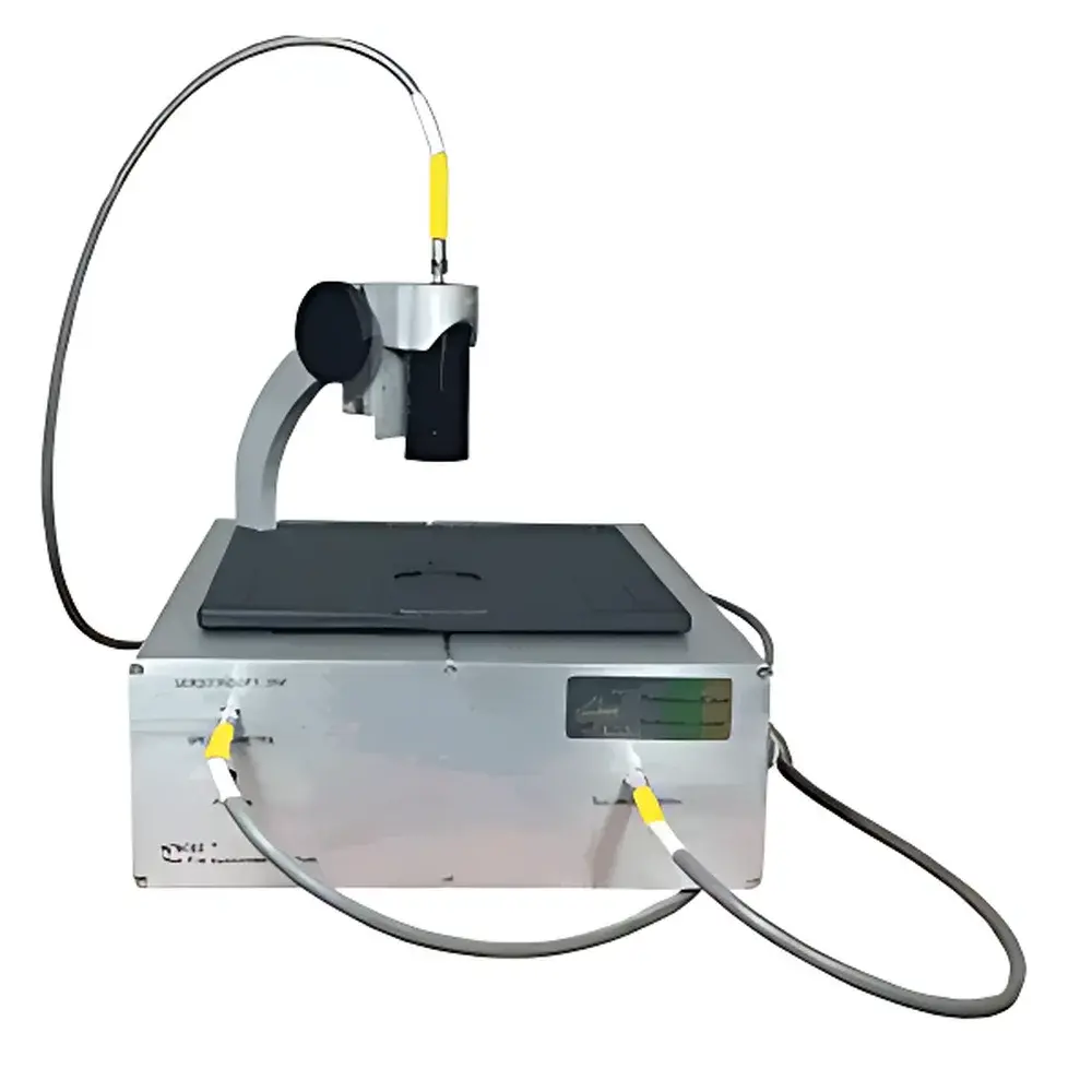
The Auniontech Mprobe 20 Single-Point Thin-Film Metrology System is a benchtop optical instrument engineered for rapid, non-contact, and non-destructive measurement of thin-film thickness and refractive index using spectral reflectometry. It operates on the physical principle of interference analysis in reflected light spectra: when broadband light illuminates a thin film on a substrate, constructive and destructive interference patterns arise due to phase shifts at each interface. By fitting the measured reflectance spectrum to a multi-layer optical model (e.g., air/film/substrate), the system solves for film thickness, complex refractive index (n + ik), and interfacial roughness with high reproducibility. Designed for routine QC labs, R&D cleanrooms, and university optics facilities, the Mprobe 20 delivers sub-nanometer resolution on single-layer dielectrics (e.g., SiO₂, Si₃N₄, Al₂O₃, ITO, polymer films) and supports up to five-layer stack analysis without sample preparation or vacuum requirements.
Key Features
- Modular optical architecture with interchangeable spectrometers and light sources—enabling configuration-specific optimization for UV-VIS, VIS-NIR, or wideband 200–1700 nm coverage
- Integrated microprocessor-controlled hardware platform including stabilized broadband illumination, fiber-coupled reflection probe, precision XYZ sample stage (SH200A), and auto-focus lens assembly
- Sub-1 mm optical spot size with manual fine-adjustment capability, suitable for localized metrology on patterned wafers, coated glass, flexible substrates, and microfluidic devices
- Factory-calibrated reference standards included: bare silicon wafers, fused silica plates, and aluminum mirrors—traceable to NIST-maintained optical constants
- Real-time spectral acquisition (< 100 ms per scan) and model-based fitting engine delivering results in under 3 seconds per measurement point
- Rugged mechanical design compliant with ISO 14644-1 Class 5 cleanroom handling; 24 VDC power supply compatible with global mains (110/220 V AC input)
Sample Compatibility & Compliance
The Mprobe 20 accommodates rigid and semi-flexible substrates ≥ 10 mm in diameter or edge length, including silicon, glass, sapphire, quartz, stainless steel, and PET. It measures transparent, semi-transparent, and weakly absorbing films—such as oxides, nitrides, fluoropolymers, photoresists, and organic semiconductor layers—without requiring conductive coatings or vacuum environments. The system conforms to key international standards governing optical thin-film characterization: ASTM E1936 (Standard Guide for Spectroscopic Ellipsometry and Reflectometry), ISO 15630-3 (Reinforcing steels and prestressing steels — Test methods — Part 3: Determination of coating thickness), and supports traceability frameworks aligned with ISO/IEC 17025. Optional software modules enable 21 CFR Part 11-compliant electronic signatures, user access control, and full audit trail logging for regulated pharmaceutical and medical device manufacturing environments.
Software & Data Management
TFCompanion-RA is the native Windows-based application that controls hardware operation, acquires spectral data, performs optical modeling, and exports metrology reports in CSV, PDF, and XML formats. Its intuitive interface allows users to define multi-layer stack models, assign wavelength-dependent dispersion relations (Cauchy, Sellmeier, Tauc-Lorentz), and apply constraints (e.g., fixed n/k values, thickness correlations between layers). Batch measurement mode supports automated XY mapping across predefined grids. Raw spectra and fitted parameters are stored with metadata (timestamp, operator ID, instrument serial number, calibration status). Data export APIs facilitate integration into LIMS and MES platforms. All software licenses are activated via USB dongle or network license server; version history and patch updates are provided through Auniontech’s secure customer portal.
Applications
- Process monitoring of PECVD, sputtering, ALD, spin-coating, and evaporation deposition lines
- Quality assurance of anti-reflective, hard-coat, and touch-sensor stacks on display cover glass
- Characterization of passivation layers in photovoltaic cell fabrication (SiNx on c-Si, Al₂O₃ on PERC)
- Thickness uniformity mapping of OLED encapsulation barriers and flexible barrier films
- Research-grade optical constant extraction for novel 2D materials (MoS₂, h-BN) and perovskite thin films
- Evaluation of degradation kinetics in biodegradable polymer coatings under environmental stress testing
FAQ
What is the minimum measurable thickness, and how is it determined?
The lower detection limit depends on both optical contrast and signal-to-noise ratio. For high-index-contrast systems (e.g., SiO₂ on Si), the Mprobe 20 reliably resolves films down to 1 nm using UV-VIS configurations with deuterium/tungsten-halogen sources and back-thinned CCD detectors. Below 5 nm, measurement uncertainty increases due to surface roughness and interfacial diffusion effects.
Can the system measure absorbing or metallic films?
Yes—within limits. Films with extinction coefficient k > 0.1 (e.g., Ti, Cr, NiCr, amorphous Si) can be modeled if their optical constants are known or pre-characterized. For highly reflective metals (Ag, Al), thickness accuracy degrades above ~30 nm due to skin-depth limitations; ellipsometry is recommended for such cases.
Is vacuum or nitrogen purging required for UV measurements?
Not for standard operation. The UV-VIS (200–1100 nm) configuration uses a sealed, purged optical path within the spectrometer housing. Ambient oxygen absorption bands below 200 nm are not accessible; no external purge gas connection is needed.
How often must the system be recalibrated?
Factory calibration remains stable for ≥12 months under typical lab conditions (23 ± 2 °C, < 50% RH, vibration-isolated bench). Annual verification using supplied reference standards (Si wafer, quartz plate) is recommended. Drift monitoring is automated via daily startup checks embedded in TFCompanion-RA.


