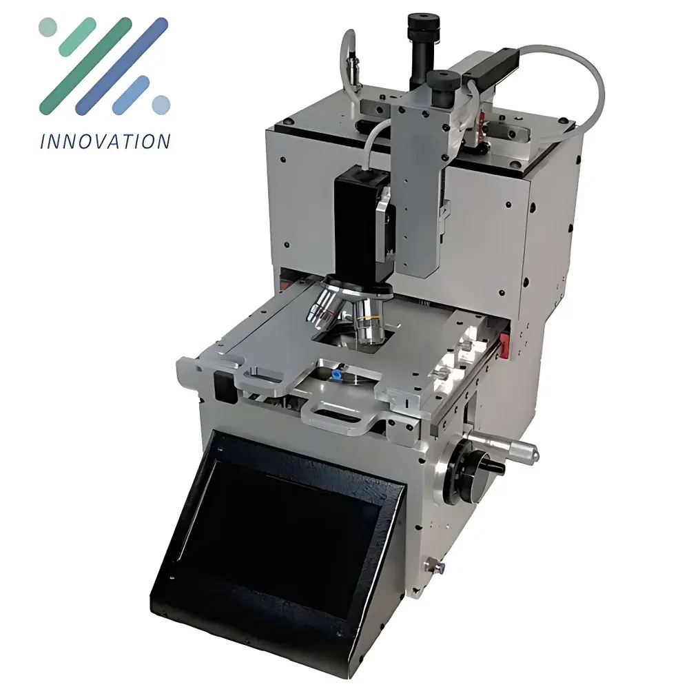
MICROTECH microAligner Desktop Mask Aligner
| Brand | MICROTECH |
|---|---|
| Origin | Netherlands |
| Manufacturer Type | Authorized Distributor |
| Origin Category | Imported |
| Model | microAligner |
| Exposure Mode | Projection-Based |
| Resolution | 100 nm |
| Light Source | High-Power UV LED |
| Wavelength | 365 nm |
| Illumination Uniformity | ≥95% |
| Maximum Exposure Area | 100 mm diameter |
| Alignment System | Coaxial Full-HD Digital Microscope with Real-Time Overlay |
| Wafer Handling | Motorized Z-Stage with Precision Gap & Contact Pressure Control |
| Alignment Stage | Micrometer-Driven XYR Manual Stage |
| Objective Lenses | Interchangeable Multi-Magnification Lens Set |
Overview
The MICROTECH microAligner Desktop Mask Aligner is a compact, high-precision projection lithography system engineered for academic research laboratories, pilot-line semiconductor fabrication facilities, and advanced materials development centers. Operating on the principle of contactless proximity/projection alignment, the microAligner utilizes a collimated 365 nm UV LED source to transfer patterns from a photomask onto photosensitive substrates—typically silicon wafers, glass, or flexible polymer films—without physical mask-to-wafer contact. Unlike laser direct-write systems that serially scan features pixel-by-pixel, this aligner employs parallel exposure over a full 100 mm circular field, delivering throughput advantages while maintaining sub-100 nm resolution under optimized process conditions. Its design emphasizes metrological stability, optical fidelity, and operational repeatability—critical requirements for mask-based lithographic processes in R&D environments where traceability, process documentation, and compliance-readiness are increasingly mandated.
Key Features
- Stable 365 nm UV LED illumination source with >10,000-hour lifetime—eliminates warm-up delays, mercury lamp degradation, and ozone generation associated with traditional Hg-vapor sources.
- Optical projection column featuring low-divergence beam path and integrated homogenizer, achieving ≥95% illumination uniformity across the full 100 mm exposure field (per ISO 10110-3).
- Coaxial full-HD digital microscope (1080p) with real-time overlay capability—enables simultaneous viewing of mask and substrate fiducials, supporting both global and local alignment strategies with sub-micron registration accuracy.
- Motorized Z-stage with closed-loop position feedback, enabling precise control of gap distance (1–50 µm) and contact pressure (0.1–5 N adjustable), critical for proximity-mode exposure consistency and defect minimization.
- Micrometer-driven XYR manual alignment stage with vernier scales (resolution: 1 µm linear, 0.01° rotational), calibrated against NIST-traceable standards and compatible with standard wafer chucks (4″, 6″, and custom substrates).
- Modular objective lens turret accommodating interchangeable magnifications (5×, 10×, 20×) to support varying alignment precision needs—from coarse die-level placement to fine-grained feature registration.
Sample Compatibility & Compliance
The microAligner supports rigid and semi-rigid substrates up to 100 mm in diameter and 5 mm in thickness, including silicon, fused silica, sapphire, quartz, ITO-coated glass, and polyimide-based flexible carriers. It accommodates standard photomasks (quartz or soda-lime glass, chrome or NiCr opaque layers) with frame sizes up to 125 × 125 mm. The system meets essential electromagnetic compatibility (EMC) requirements per EN 61326-1 and safety standards per IEC 61010-1. While not certified as a GMP production tool, its mechanical repeatability (σ < 0.3 µm over 50 alignments), documented calibration procedures, and audit-ready operation logs enable use in GLP-compliant workflows. Process parameters—including exposure dose (J/cm²), gap setting, and alignment coordinates—are digitally recorded and exportable for internal quality review or regulatory submission preparation.
Software & Data Management
The microAligner operates via a dedicated Windows-based control interface with intuitive wizard-guided workflows for alignment, exposure sequencing, and parameter logging. All alignment steps—including fiducial detection, offset calculation, and stage correction—are timestamped and stored in structured CSV/JSON format. Exposure dose is calculated in real time using calibrated radiometric feedback from an integrated photodiode sensor referenced to NIST-traceable UV irradiance standards. Audit trail functionality records user ID, timestamp, parameter changes, and execution status—supporting alignment with FDA 21 CFR Part 11 principles for electronic records and signatures when deployed in regulated development settings. Raw image data from the alignment microscope is saved losslessly (TIFF), enabling post-hoc verification and metrology traceability.
Applications
- Prototyping of MEMS devices, microfluidic chips, and optoelectronic interposers requiring multi-layer registration accuracy.
- R&D-scale fabrication of organic thin-film transistors (OTFTs), perovskite solar cells, and resistive switching memory arrays.
- Mask-based patterning for plasmonic nanostructures, diffractive optical elements (DOEs), and surface acoustic wave (SAW) sensors.
- Teaching platforms in microfabrication courses—providing hands-on experience with photolithography fundamentals without cleanroom-grade infrastructure.
- Hybrid integration processes combining photolithography with inkjet printing, aerosol jet deposition, or laser annealing.
FAQ
What is the minimum feature size achievable with the microAligner under standard process conditions?
Under optimal resist selection (e.g., Shipley S1813), focus control, and alignment stability, users routinely achieve resolved line/space patterns down to 100 nm (as verified by SEM cross-section analysis).
Does the system support automated alignment or require manual intervention?
The microAligner implements semi-automated alignment: the operator initiates fiducial search, and the software calculates correction vectors; final fine-tuning and exposure initiation remain manual to ensure process awareness and reproducibility.
Can the microAligner be integrated into a Class 1000 cleanroom environment?
Yes—the unit is designed for low particle generation (<100 particles ≥0.5 µm/m³ during operation) and includes optional HEPA-filtered exhaust ducting for seamless integration into controlled environments.
Is radiometric calibration of the UV output performed at the factory?
Each unit ships with a certificate of calibration referencing a NIST-traceable UV-A radiometer, and annual recalibration services are available through MICROTECH’s European service network.
What file formats are supported for mask alignment overlays?
The software accepts standard bitmap overlays (BMP, PNG) and vector-based alignment templates (SVG), enabling integration with CAD layout tools such as KLayout or Cadence Virtuoso.
Related Products