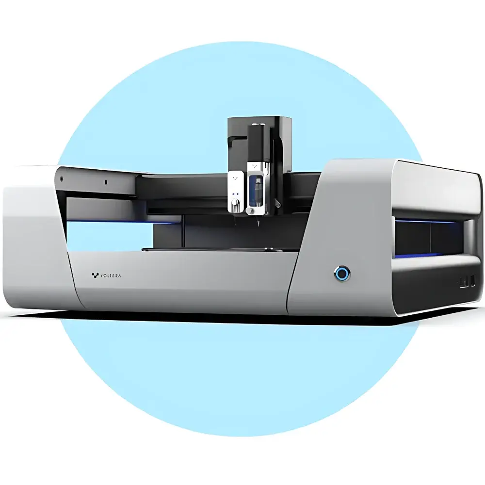
Voltera Nova High-Performance Flexible Microelectronics Printer
| Brand | Voltera |
|---|---|
| Origin | Canada |
| Model | Nova |
| Type | Maskless Additive Manufacturing System for Printed Electronics |
| Printing Technology | Precision Extrusion-Based Deposition |
| Substrate Compatibility | Rigid, Flexible, and Topographically Irregular Surfaces |
| Ink Viscosity Range | 10 mPa·s to 250,000 mPa·s |
| Positioning Accuracy | ±1.5 µm (X/Y), ±0.5 µm (Z) |
| Layer Registration Accuracy | <5 µm via Optical Stack Alignment |
| Real-Time Feedback | Closed-Loop Pressure Control + Path Tracking Sensor |
| Software Platform | V-One Desktop Suite (v4.2+) |
Overview
The Voltera Nova High-Performance Flexible Microelectronics Printer is an industrial-grade, maskless additive manufacturing platform engineered for the direct-write fabrication of functional electronic circuits, sensors, antennas, and interconnects on non-planar, flexible, and heterogeneous substrates. Unlike photolithographic or screen-printing methods, the Nova employs precision extrusion-based deposition—leveraging piezoelectrically actuated microdispensing nozzles and real-time closed-loop pressure regulation—to achieve micron-level placement fidelity without requiring masks, stencils, or vacuum environments. Its core architecture integrates optical stack alignment, dynamic path tracking, and adaptive Z-height compensation, enabling consistent layer registration across substrates with surface variations exceeding ±100 µm. Designed for R&D labs and pilot-scale production in printed electronics, the Nova bridges the gap between rapid prototyping and process-transfer-ready fabrication—supporting development workflows compliant with ISO/IEC 17025–accredited metrology practices.
Key Features
- Precision extrusion system with dual-pressure control: independent pneumatic and piezoelectric actuation enables stable dispensing across a 10–250,000 mPa·s viscosity range—from conductive nanoparticle inks to high-fill-ratio polymer composites.
- Optical stack alignment subsystem: uses calibrated machine vision to detect fiducial markers and correct for thermal drift or mechanical misalignment between layers, achieving sub-5 µm overlay accuracy over 100 mm² areas.
- Real-time path tracking feedback: integrated scanning sensor monitors nozzle-to-substrate distance and ink filament continuity during motion, triggering automatic Z-axis recalibration or pause-on-failure protocols.
- Modular toolhead interface: supports interchangeable nozzles (100–500 µm ID), heated print beds (up to 120 °C), and optional UV-curing modules for hybrid material processing.
- Robust mechanical frame: granite composite base and linear motor-driven gantry ensure vibration damping and positional repeatability better than ±1.5 µm over extended duty cycles.
Sample Compatibility & Compliance
The Nova accommodates substrates up to 200 × 200 mm, including polyimide (Kapton®), PET, paper, textile laminates, elastomeric PDMS, and ceramic-coated metal foils. It maintains uniform line resolution (typical width: 80–150 µm) on surfaces with curvature radii down to 5 mm and step heights up to 120 µm. All firmware and motion control logic comply with IEC 61508 SIL2 functional safety requirements. The system’s software audit trail—including user login timestamps, parameter versioning, and raw sensor log export—supports GLP/GMP-aligned documentation per FDA 21 CFR Part 11 when configured with network authentication and encrypted local storage.
Software & Data Management
The V-One Desktop Suite (v4.2+) provides CAD-native import (Gerber, DXF, SVG), multi-layer alignment preview, and parametric print recipe management. Each job file embeds full metadata: nozzle calibration history, pressure ramp profiles, ambient temperature/humidity logs, and optical alignment confidence scores. Export formats include CSV (sensor telemetry), HDF5 (raw imaging data), and PDF reports with embedded traceability QR codes. Remote monitoring via HTTPS-secured WebSocket API enables integration into LabVantage or Thermo Fisher SampleManager LIMS environments. Firmware updates undergo SHA-256 signature verification and are delivered through Voltera’s ISO 27001-certified update infrastructure.
Applications
- Rapid iteration of stretchable bioelectrodes for wearable ECG/EMG systems, printed directly onto silicone membranes with conformal adhesion.
- Functionalization of MEMS packaging substrates: localized deposition of silver epoxy for RF shielding traces without thermal damage to underlying die.
- Multi-material integration in smart labels: sequential printing of antenna loops (Ag nanowire ink), dielectric barriers (PVDF-TrFE), and resistive sensing elements (carbon-black/PEDOT:PSS).
- Academic microfabrication: teaching platforms for printed thermoelectrics, electrochromic displays, and low-cost RFID tag prototyping under cleanroom-adjacent conditions.
- Process qualification for ISO 13485 medical device manufacturers: generating DoE-compliant print logs for design transfer to roll-to-roll production lines.
FAQ
What substrate flatness tolerance does the Nova support without manual leveling?
The system automatically compensates for Z-variance up to ±120 µm across the build area using real-time optical height mapping prior to each layer—no manual shimming required.
Can the Nova print conductive traces compatible with solder reflow processes?
Yes—silver, copper, and nickel nanoparticle inks validated by Voltera achieve >1×10⁶ S/m conductivity post-sintering at 150 °C (N₂ atmosphere), with solder wettability confirmed per IPC-J-STD-004B Annex A.
Is remote diagnostics supported for troubleshooting in regulated lab environments?
All diagnostic telemetry (motor current waveforms, pressure transducer noise floor, camera focus metrics) is logged locally and can be exported as encrypted ZIP archives for off-site engineering review—no cloud transmission occurs by default.
Does the system meet electromagnetic compatibility requirements for use near MRI or SEM facilities?
The Nova complies with CISPR 11 Group 1 Class B emission limits and IEC 61000-4-2/3/4/6 immunity standards; optional ferrite-shielded cabling kits are available for ultra-low-noise operation.