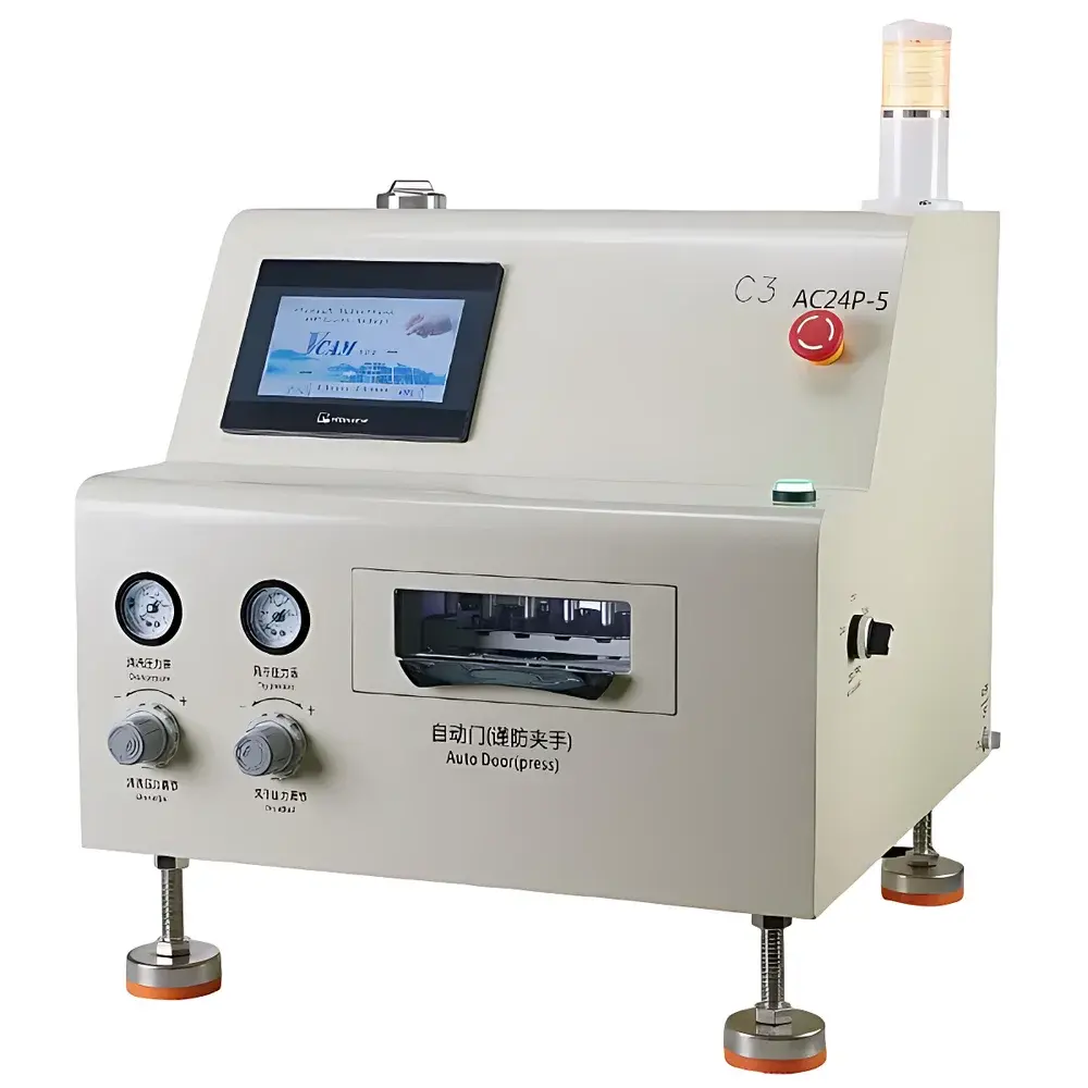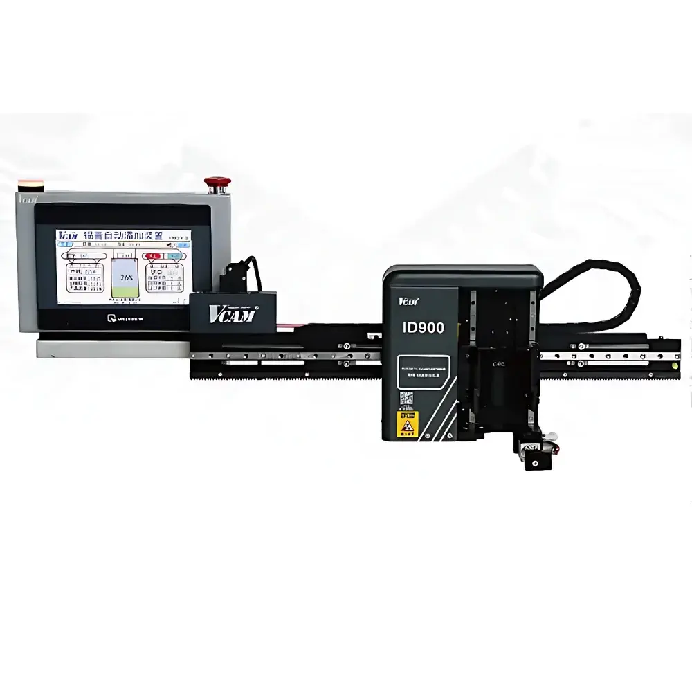
Nanoprintek Multi-Material Laser-Induced Dry Printing System
| Brand | Nanoprintek |
|---|---|
| Origin | USA |
| Manufacturer Type | Authorized Distributor |
| Product Origin | Imported |
| Model | Nanoprintek Multi-Material Printer |
| Application Field | Rapid Prototyping of Microelectronic Circuits |
| Compatible Materials | Metals, Insulators, Semiconductors, Ceramics, Oxides, Nitrides, Carbides, Borides, Silicides, Sulfides, Halides, and Fluorides |
Overview
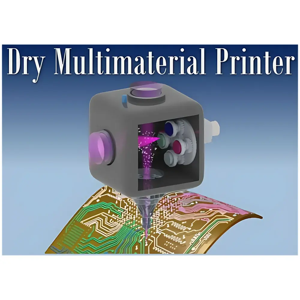
The Nanoprintek Multi-Material Laser-Induced Dry Printing System is a precision microscale additive manufacturing platform engineered for direct-write fabrication of functional electronic devices without solvents, binders, or pre-synthesized inks. Unlike conventional wet-process printing methods—such as inkjet, aerosol jet, or screen printing—the system employs a proprietary laser-induced dry material transfer mechanism that integrates pulsed laser deposition (PLD) principles with maskless spatial patterning. A high-repetition-rate UV or deep-UV pulsed laser (e.g., KrF excimer or frequency-tripled Nd:YAG) is focused onto solid-phase target materials in vacuum or controlled inert atmosphere, generating transient plasma plumes composed of stoichiometric nanoclusters and atomic species. These plumes are directionally deposited onto substrates with sub-micron registration accuracy, enabling in situ synthesis of phase-pure nanostructured films—including metals (Ag, Cu, Ni), wide-bandgap oxides (ZnO, ITO, TiO₂), perovskites, chalcogenides (MoS₂, WS₂), nitrides (Si₃N₄, AlN), and biodegradable metal fluorides (MgF₂, CaF₂). The process eliminates solvent drying, thermal decomposition, and post-annealing steps, preserving stoichiometry and interfacial integrity—particularly critical for stretchable, transient, and ultra-thin electronics.
Key Features
- Laser-induced dry transfer architecture: No liquid carriers, no binder removal, no nanoparticle agglomeration or oxidation during processing
- Multi-material co-printing capability: Sequential or simultaneous ablation from up to 8 independently controlled solid targets under programmable laser fluence and repetition rate
- Sub-5 µm lateral resolution with <10 nm film thickness control (measured via in situ quartz crystal microbalance and ex situ XRD/XPS validation)
- Compatible with low-glass-transition, non-planar, and bioresorbable substrates—including PDMS, PI, PET, cellulose paper, Mg alloys, and polylactic acid (PLA)
- Integrated high-vacuum chamber (<1×10⁻⁶ Torr) with residual gas analysis (RGA) and real-time plasma diagnostics (OES)
- Programmable beam shaping optics supporting line scanning, spot rastering, and dynamic focus modulation for 3D topography adaptation
Sample Compatibility & Compliance
The system supports heterogeneous integration across rigid, flexible, stretchable, and transient substrate classes. It has been validated for use with ISO 10993-compliant biodegradable polymers, ASTM F2129-certified corrosion-resistant metallic foils, and USP Class VI medical-grade elastomers. Process parameters are traceable and auditable per FDA 21 CFR Part 11 requirements when configured with optional electronic logbook and user-role-based access control. All vacuum and laser safety subsystems comply with ANSI Z136.1 (laser safety) and ISO 20471 (vacuum equipment safety). Material deposition protocols align with ASTM F3049–22 (standard guide for characterization of printed electronics) and IEC 62753 (requirements for flexible hybrid electronics).
Software & Data Management
Controlled via Nanoprintek’s proprietary PrintFlow™ software suite, the system provides CAD-to-print workflow integration with native support for G-code, Gerber RS-274X, and ODB++ formats. Real-time monitoring includes laser energy calibration logs, plume intensity mapping, chamber pressure history, and substrate temperature profiling—all timestamped and exportable in CSV/JSON. Audit trails meet GLP/GMP documentation standards, including full operator attribution, parameter versioning, and immutable session records. Optional API integration enables linkage with LIMS platforms (e.g., LabVantage, Thermo Fisher SampleManager) and MES systems for production traceability in pilot-line environments.
Applications
- Rapid prototyping of hybrid flexible circuits combining conductive traces, dielectric passivation, and semiconductor active layers on single substrates
- Fabrication of transient biosensors with Mg/Zn-based electrodes and SiO₂/PCL encapsulation for implantable diagnostics
- On-demand deposition of LiCoO₂, LiFePO₄, or solid-state sulfide electrolytes for microbattery architectures with >95% volumetric utilization
- Direct-write fabrication of piezoelectric MEMS elements (e.g., AlN or ZnO cantilevers) on CMOS wafers without back-end-of-line thermal budget constraints
- Functionalization of aerospace-grade polyimide films with radiation-hardened metal-oxide heterostructures for in-situ structural health monitoring
- Deposition of superconducting NbN or MgB₂ thin films on silicon photonics platforms for cryogenic integrated quantum circuits
FAQ
Does the system require pre-synthesized nanoparticle inks?
No. The Nanoprintek platform operates exclusively with solid-phase targets; nanoparticles are generated in situ via laser ablation and deposited directly without colloidal stabilization or surfactants.
Can it print on curved or 3D surfaces?
Yes—when equipped with optional motorized tilt-stage and adaptive focus compensation, the system achieves uniform deposition on substrates with radii of curvature down to 5 mm.
Is process repeatability validated across multiple labs?
Yes. Inter-laboratory round-robin studies conducted under NIST-led protocols (IR 8362) demonstrated ≤3.2% RSD in sheet resistance for Ag lines (10 µm width) across five independent installations.
What vacuum level is required for oxide deposition?
For stoichiometric oxide transfer (e.g., ITO, ZnO), base pressure ≤5×10⁻⁷ Torr with 1–10 mTorr O₂ partial pressure is recommended; nitrogen or argon ambient suffices for metals and nitrides.
Is training and application support included?
Yes—Nanoprintek provides on-site installation qualification (IQ), operational qualification (OQ), and comprehensive user certification programs aligned with ISO/IEC 17025 competency frameworks.
Related Products