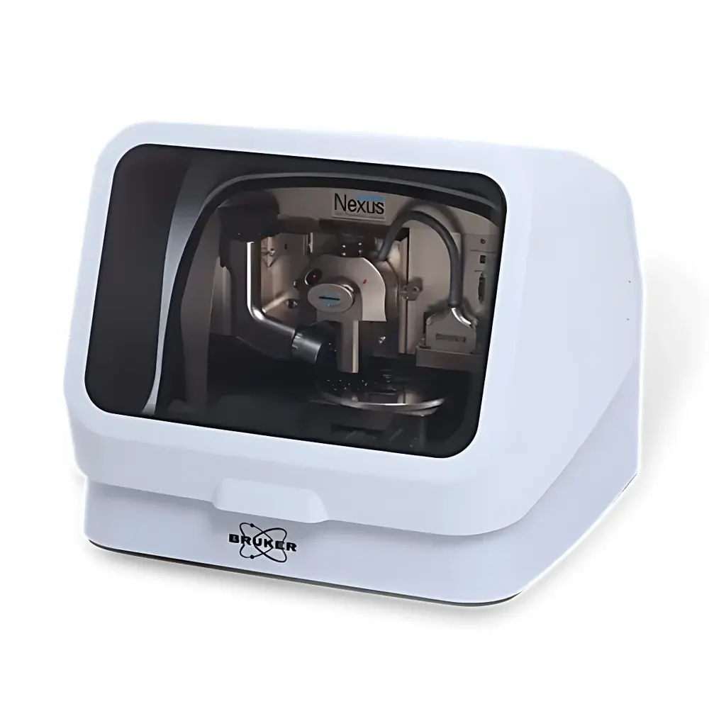
Bruker Dimension Nexus Atomic Force Microscope
| Brand | Bruker |
|---|---|
| Origin | Germany |
| Manufacturer Type | Authorized Distributor |
| Origin Category | Imported |
| Model | Dimension Nexus AFM |
| Instrument Type | Atomic Force Microscope |
| Maximum Sample Size | 200 mm |
Overview
The Bruker Dimension Nexus Atomic Force Microscope (AFM) is an advanced, open-access scanning probe microscopy platform engineered for high-resolution topographic, mechanical, electrical, and chemical property mapping across diverse material classes. Operating on the fundamental principle of nanomechanical force detection—where a sharp probe raster-scans a surface while monitoring cantilever deflection, oscillation amplitude, or phase—the Dimension Nexus leverages Bruker’s proprietary PeakForce Tapping® technology to achieve true quantitative nanoscale characterization with sub-nanometer resolution and piconewton force control. Unlike conventional contact or tapping-mode AFMs, PeakForce Tapping decouples imaging from property measurement by applying controlled, low-noise force modulation at kHz frequencies, enabling simultaneous acquisition of height, adhesion, deformation, modulus, and dissipation maps—without tip wear or sample damage. The system integrates a next-generation NanoScope 6 controller featuring ultra-low electronic noise floor (<100 fA RMS), real-time 125 MHz data throughput, and deterministic latency for closed-loop feedback stability—critical for long-duration, large-area metrology and time-resolved studies.
Key Features
- PeakForce Tapping® mode with full quantitative nanomechanical property mapping (elastic modulus, adhesion, deformation, dissipation)
- NanoScope 6 controller with hardware-accelerated real-time processing, 16-bit DAC/ADC, and integrated FPGA for sub-millisecond loop response
- XYZ closed-loop scanner with bridge-type granite base and offset-compensated piezoelectric actuation—enabling <0.1 nm RMS thermal drift over 2 hours and zero scan artifacts across 90 µm × 2 µm fields of view
- Open-access probe–sample interface: physically unobstructed stage with standardized mounting points for custom electrical, optical, or environmental accessories
- Programmable high-throughput stage supporting automated multi-location acquisition, grid-based metrology, and batch analysis workflows
- ScanAsyst® auto-optimization suite: intelligently configures probe approach, setpoint, gain, and scan parameters based on real-time signal statistics—reducing operator dependency and improving inter-user reproducibility
Sample Compatibility & Compliance
The Dimension Nexus accommodates samples up to 200 mm in diameter—including wafers, thin films, polymers, biological specimens (on mica or silicon substrates), and heterogeneous composites—without requiring vacuum or conductive coating. Its modular environmental enclosure options support inert-gas purging, humidity control (5–95% RH), and temperature regulation (−30 °C to +200 °C). The platform complies with ISO/IEC 17025 calibration traceability requirements for metrological AFM applications and supports audit-ready data logging aligned with GLP and FDA 21 CFR Part 11 principles when paired with Bruker’s NanoScope Analysis software with electronic signature and version-controlled report generation.
Software & Data Management
NanoScope Analysis v9.1 provides a comprehensive, scriptable environment for post-processing, statistical analysis, and dimensional metrology—including line profile extraction, power spectral density (PSD) calculation, grain analysis, and critical dimension (CD) metrology per SEMI, ASTM E2492, and ISO 25178 standards. Raw data is stored in Bruker’s open-format .spm binary format, fully compatible with Python (via the pySPM library), MATLAB, and third-party tools. The NanoScope 6 controller features front-panel BNC I/O ports for synchronized external stimulus (e.g., voltage bias, laser pulses) and real-time analog output of any measured channel—enabling custom feedback loops and correlative experiments. All acquisition scripts are editable in Python or LabVIEW, and the system supports direct integration with Bruker’s Nanoscope Automation Framework for LIMS and MES connectivity.
Applications
The Dimension Nexus serves as a core metrology tool in semiconductor process development (line-edge roughness, trench depth uniformity, overlay registration), advanced materials R&D (polymer phase separation, battery electrode degradation, 2D material strain mapping), life sciences (membrane protein distribution, cell stiffness gradients, extracellular matrix remodeling), and nanomanufacturing QA/QC (nanoparticle size distribution, anti-reflective coating homogeneity, MEMS device actuation fidelity). Its ability to resolve sub-1 nm features on soft biological samples—while quantifying local Young’s modulus with ±5% repeatability—makes it uniquely suited for cross-disciplinary labs requiring both structural and functional nanoscale insight.
FAQ
What sample preparation is required for non-conductive samples?
No metallization or charge-dissipative coating is necessary. PeakForce Tapping operates effectively on insulating surfaces—including oxides, polymers, and biological tissues—by eliminating electrostatic charging artifacts common in traditional tapping modes.
Can the system perform in situ electrical measurements?
Yes—via optional conductive probes (e.g., SCM-PIT, CSG01) and integrated current amplifiers, the Dimension Nexus supports current–voltage spectroscopy, surface potential mapping (KPFM), and nanoscale conductivity profiling with picoampere sensitivity.
Is remote operation supported for shared facility use?
Fully supported via Bruker’s NanoRemote client, enabling secure, role-based access to instrument control, live imaging, and data review from off-site locations—compliant with institutional IT security policies and FERPA/HIPAA data handling guidelines.
How does the system ensure long-term dimensional stability during overnight scans?
Through active thermal compensation algorithms embedded in the NanoScope 6 firmware, coupled with the granite-isolated bridge scanner and passive air-damping enclosure—achieving <0.05 nm/min vertical drift rate under ambient lab conditions.
Are calibration standards traceable to NIST or PTB?
Yes—Bruker provides certified reference samples (e.g., TGT01 grating, Si grating SRM 2053) with NIST-traceable pitch and step-height values, and all system calibrations are documented per ISO/IEC 17025 Annex A.2 requirements.


