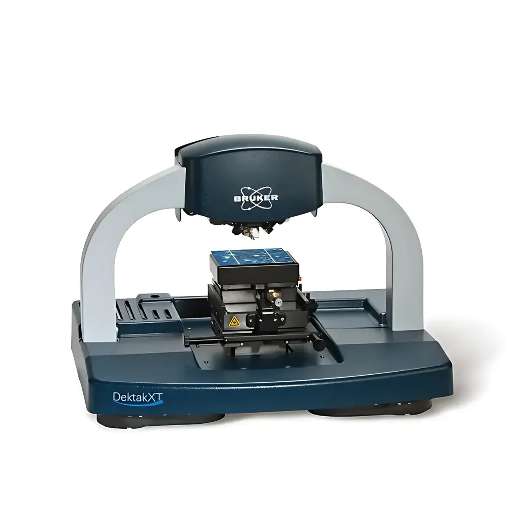
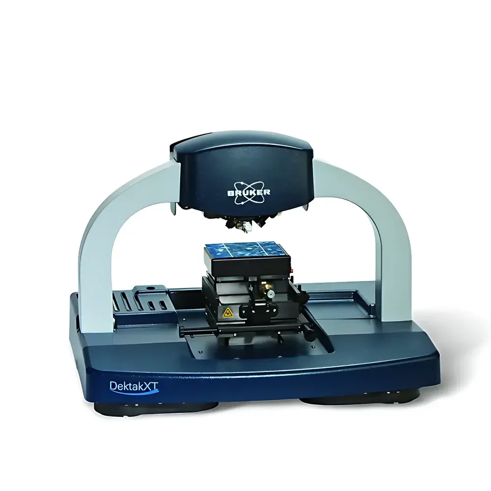
Bruker Dektak XT Stylus Profilometer
| Brand | Bruker |
|---|---|
| Origin | Germany |
| Manufacturer Type | Authorized Distributor |
| Product Origin | Imported |
| Model | Dektak XT |
| Measurement Principle | Capacitive Sensing |
| Measurement Capability | 2D Surface Topography Profiling |
| Vertical Accuracy | ±1 Å |
| Probe Tip Radius | 50 nm – 25 µm |
| Normal Force | 15 µN |
| Scan Length | 55 mm (2 inch) |
| Step Height Repeatability | <5 Å |
| Vertical Resolution | 1 Å |
| Maximum Sample Size | 50 mm |
Overview
The Bruker Dektak XT is a high-precision, capacitive-based stylus profilometer engineered for nanoscale step height and surface topography characterization. Leveraging over four decades of Dektak platform evolution, the XT represents the tenth-generation advancement in contact-mode profilometry—designed specifically to meet stringent metrology requirements in semiconductor process development, thin-film R&D, MEMS fabrication, photovoltaic layer analysis, and advanced materials science. Its core measurement principle relies on a precisely controlled, low-force capacitive sensor that detects vertical displacement of a diamond-tipped stylus as it traverses a sample surface. This enables quantitative profiling of features ranging from sub-nanometer roughness to multi-micron steps—without optical diffraction limits or signal ambiguity associated with non-contact methods. The system’s monolithic single-arch mechanical architecture minimizes structural compliance and vibration coupling, while upgraded intelligent electronics actively compensate for thermal drift and environmental noise—ensuring stable, repeatable operation under standard laboratory conditions.
Key Features
- Direct-drive scanning stage reduces measurement time by up to 40% versus previous generations, enabling rapid acquisition of high-density profile data across full 55 mm scan lengths.
- Sub-ångström vertical resolution (1 Å) and exceptional step height repeatability (<5 Å) validated per ISO 25178-6 and ASTM E1316 standards for surface texture metrology.
- Modular, self-aligning probe assembly allows tool-free, repeatable probe exchange—eliminating alignment uncertainty and reducing operator-induced variability.
- Adjustable normal force (down to 15 µN) and wide-range probe tip radii (50 nm – 25 µm) support characterization of soft polymers, brittle oxides, and ultra-thin films without damage or ploughing artifacts.
- Integrated thermal management and low-noise analog front-end electronics ensure long-term stability and minimal baseline drift—critical for extended automated runs and GLP-compliant workflows.
Sample Compatibility & Compliance
The Dektak XT accommodates substrates up to 50 mm in diameter—including bare wafers, patterned silicon, glass, sapphire, flexible polymer films, and coated medical device components. Its open-stage design permits custom fixturing for irregular geometries and edge-profile measurements. All hardware and software comply with ISO/IEC 17025 traceability frameworks, and system validation protocols align with SEMI MF1529 (for semiconductor wafer metrology) and USP (analytical instrument qualification). Audit trails, electronic signatures, and user-access controls within Vision64 support FDA 21 CFR Part 11 compliance for regulated environments.
Software & Data Management
Vision64 is Bruker’s native 64-bit parallel processing platform—optimized for large-volume 3D topography datasets and real-time multi-region analysis. It supports batch processing of hundreds of scans with customizable scripting (via Python API), automated pass/fail decision logic based on user-defined thresholds, and export of metrology reports compliant with ISO 25178-2 surface parameters (Sa, Sq, Sz, etc.). Raw profile data is stored in vendor-neutral ASCII formats; metadata—including calibration history, environmental logs, and operator annotations—is embedded directly into each file. Version-controlled analysis templates enable method transfer between labs and ensure inter-instrument comparability across global manufacturing sites.
Applications
- Semiconductor: Gate oxide thickness uniformity, CMP endpoint detection, trench depth metrology, and lithographic resist profile analysis.
- LED & Display: Quantum dot layer thickness, ITO electrode step coverage, and micro-LED mesa etch depth verification.
- Photovoltaics: Anti-reflective coating step heights, textured Si surface roughness quantification, and perovskite film morphology assessment.
- Biomedical: Drug-eluting stent coating thickness, hydrogel swelling kinetics, and microfluidic channel depth mapping.
- Advanced Materials: 2D material flake thickness (graphene, MoS₂), ALD film growth rate monitoring, and tribological wear track profiling.
FAQ
What is the minimum measurable step height with the Dektak XT?
The system achieves reliable quantification of steps down to <10 Å under optimized conditions, supported by its 1 Å vertical resolution and <5 Å repeatability specification.
Can the Dektak XT measure curved or non-planar samples?
Yes—optional motorized tilt and Z-height compensation modules allow accurate profiling of gently curved surfaces (e.g., lens substrates, wafer bow), provided curvature radius exceeds 500 mm.
Is Vision64 compatible with third-party data analysis tools?
All raw profile data exports in standardized ASCII format with header metadata, enabling direct import into MATLAB, Python (NumPy/Pandas), or commercial statistical packages such as JMP or Minitab.
How does the Dektak XT handle vibration-sensitive environments?
The monolithic arch frame, combined with active inertial damping in the drive electronics, provides inherent immunity to broadband floor vibrations—no external air tables required for routine operation.
What calibration standards are recommended for routine verification?
Bruker recommends NIST-traceable step height standards (e.g., VLSI Standards S100 series) and certified roughness specimens (e.g., ISO 25178 reference blocks) for daily performance checks and periodic requalification.