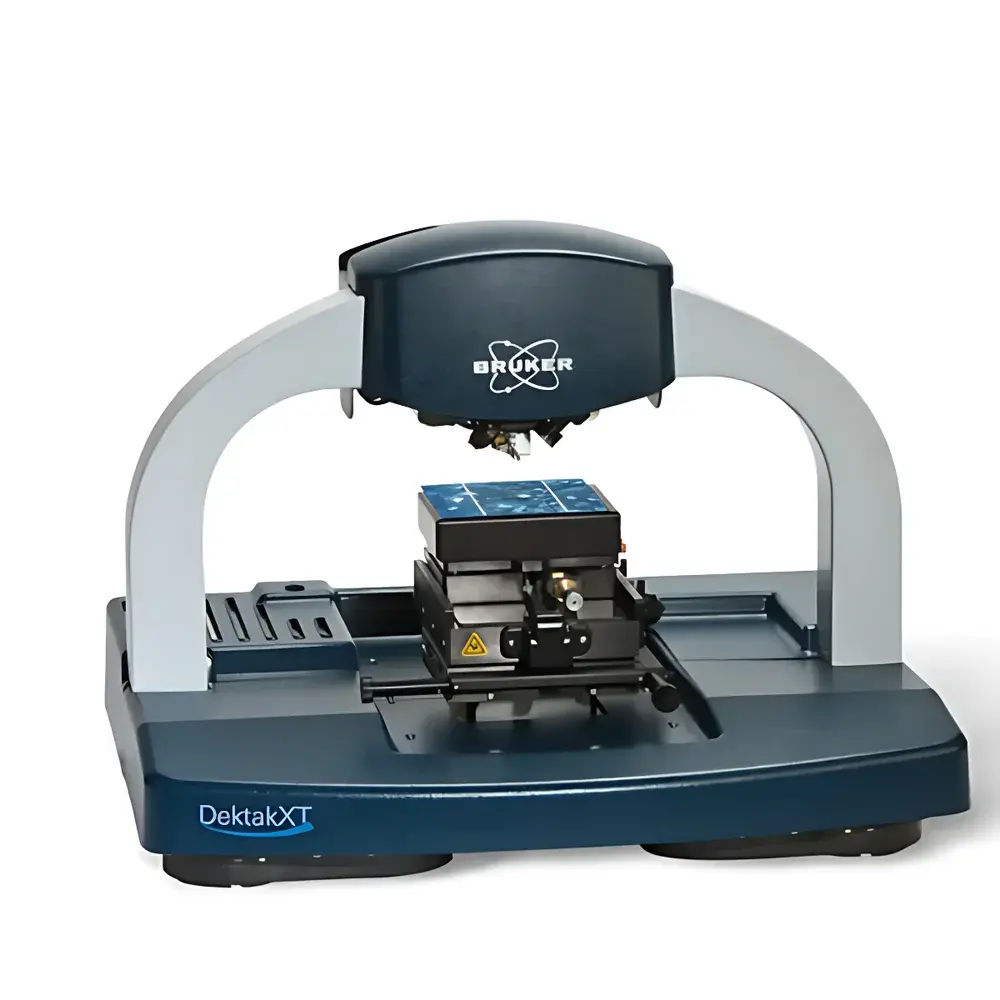
Bruker Dektak XT Stylus Profilometer
| Brand | Bruker |
|---|---|
| Origin | USA |
| Model | XT |
| Measurement Principle | Capacitive |
| Measurement Modes | 2D Surface Profiling (standard), Optional 3D Profiling & Advanced Data Analysis |
| Probe Tip Radius | 50 nm – 25 µm |
| Normal Force Range | 1–15 mg (LIS3 sensor) |
| Scan Length | 55 mm (2 in) |
| Step Height Repeatability | <5 Å (1σ on 0.1 µm step) |
| Vertical Scan Range | 1 mm |
| Vertical Resolution | 1 Å (within 6.55 µm full-scale range) |
| Maximum Sample Thickness | 50 mm |
| Wafer Compatibility | Up to 200 mm (8 in) |
| X/Y Stage Options | Manual (100 × 100 mm, 4 in) or Motorized (150 × 150 mm, 6 in), both with manual leveling and 360° continuous rotation |
| Optical View | Integrated true-color HD camera, FOV 1–4 mm |
| Data Points per Scan | Up to 120,000 |
| Software Platform | Vision64 (64-bit parallel processing), includes stress measurement, cantilever deflection, stitching, and 3D analysis modules (optional) |
| Operating Environment | 20–25 °C, ≤80% RH (non-condensing) |
| Power | 100–240 VAC, 50–60 Hz |
| System Dimensions (W×D×H) | 455 × 550 × 370 mm |
| Weight | 34 kg (excl. isolation enclosure) |
Overview
The Bruker Dektak XT is a high-precision, capacitive-based stylus profilometer engineered for nanoscale surface topography characterization. It operates on the principle of mechanical contact between a diamond-tipped probe and the sample surface, where vertical displacement of the probe—detected via a low-inertia capacitive transducer—is converted into high-fidelity height data. This direct-contact methodology enables quantitative measurement of step heights, surface roughness (Ra, Rq, Rz), film thickness (via step-edge profiling), and thin-film stress (using curvature analysis). With a certified step height repeatability of <5 Å (1σ on a 0.1 µm step) and vertical resolution down to 1 Å within a 6.55 µm measurement range, the Dektak XT meets stringent metrology requirements in semiconductor process development, MEMS fabrication, battery electrode characterization, and advanced optoelectronic materials research. Its single-arch mechanical architecture minimizes thermal drift and mechanical hysteresis, ensuring long-term stability across multi-hour measurement campaigns.
Key Features
- Single-arch structural design delivering exceptional scanning stability and reduced vibration sensitivity over extended scan lengths (up to 55 mm)
- Low-Inertia Sensor 3 (LIS3) with programmable normal force control (1–15 mg standard; 0.03–15 mg with N-Lite+ mode) for delicate or compliant surfaces
- Integrated true-color HD optical camera with selectable magnification and 1–4 mm field-of-view for precise probe positioning and feature identification
- Direct-drive scanning platform enabling 40% faster data acquisition without compromising resolution or noise floor
- 64-bit Vision64 software with real-time parallel data processing—accelerating 3D reconstruction, filtering, and multi-scan stitching by up to 10× versus legacy platforms
- Automated tip calibration routine ensuring consistent probe geometry registration across instrument lifetime
- Modular software suite supporting ISO 4287/4288-compliant roughness analysis, ASTM F390-22 thin-film stress calculation, and USP instrument qualification templates
Sample Compatibility & Compliance
The Dektak XT accommodates substrates from bare silicon wafers (up to 200 mm / 8 in diameter) to flexible polymer films, glass substrates, and coated battery electrodes. Its motorized X/Y stage (150 × 150 mm travel) supports full-wafer mapping with manual leveling and continuous 360° rotation for angular feature alignment. Probe options include standard radii (50 nm–25 µm), high-aspect-ratio tips (10 µm × 2 µm and 200 µm × 20 µm), and custom geometries for specialized applications such as deep trench or high-slope sidewall profiling. The system complies with ISO/IEC 17025 traceability frameworks when used with NIST-traceable step height standards, and its audit trail functionality in Vision64 satisfies FDA 21 CFR Part 11 requirements for electronic records and signatures in regulated environments (e.g., GMP-compliant QC labs).
Software & Data Management
Vision64 serves as the unified 64-bit software environment for instrument control, real-time visualization, and post-processing. It implements deterministic multithreaded acquisition—synchronizing analog signal capture, stage motion, and image overlay at hardware level—to eliminate timing jitter. Built-in analysis modules conform to ISO 25178-2 (areal surface texture) and ASTM E1077 (film thickness by stylus profilometry). Raw data is stored in HDF5 format with embedded metadata (timestamp, operator ID, calibration history, environmental logs), enabling seamless integration into LIMS or ELN systems. Optional modules include Stress Analysis (based on Stoney’s equation), Cantilever Deflection Mapping, and Large-Area Stitching—each validated per IQ/OQ protocols aligned with GLP and GMP documentation practices.
Applications
The Dektak XT is routinely deployed in R&D and production environments for quantifying critical parameters including: etch depth and deposition uniformity in CMOS and compound semiconductor processes; anode/cathode coating thickness and edge definition in Li-ion battery manufacturing; surface roughness of polished optical substrates per MIL-PRF-13830B; stress-induced curvature in thin-film photovoltaic stacks; and microfluidic channel depth profiles in lab-on-a-chip devices. Its ability to resolve sub-nanometer steps makes it indispensable for evaluating atomic layer deposition (ALD) cycle counts, self-assembled monolayer (SAM) thickness, and quantum dot layer integrity—applications where optical interferometry reaches theoretical resolution limits.
FAQ
What is the minimum resolvable step height on the Dektak XT?
The system achieves <5 Å step height repeatability (1σ) on a 0.1 µm reference step, with vertical resolution of 1 Å within a 6.55 µm full-scale range.
Can the Dektak XT perform automated wafer mapping?
Yes—when equipped with the motorized 6-inch X/Y stage and Vision64’s scripting interface, it supports programmable grid-based profiling, including auto-focus, tip approach, and multi-point averaging per site.
Is the system compatible with cleanroom environments?
The Dektak XT meets ISO Class 5 particulate requirements when operated inside optional laminar flow enclosures; its non-outgassing construction and sealed electronics minimize contamination risk.
How is traceability maintained for calibration?
Bruker provides factory-certified calibration using NIST-traceable step height standards (e.g., 10 nm–1 µm SiO₂-on-Si artifacts), with documented uncertainty budgets per ISO/IEC 17025.
Does Vision64 support automated report generation for quality audits?
Yes—templates can be configured to export PDF/Excel reports containing raw traces, statistical summaries, pass/fail flags against user-defined tolerances, and digital signatures compliant with 21 CFR Part 11.