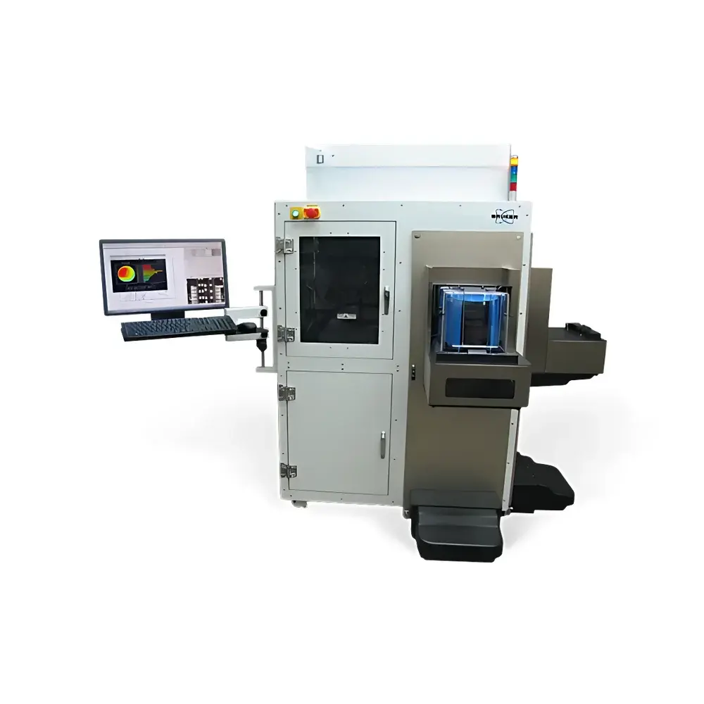
Bruker FilmTek 6000 PAR-SE Spectroscopic Ellipsometer with Multi-Angle Differential Polarimetry
| Brand | Bruker |
|---|---|
| Origin | Germany |
| Model | FilmTek 6000 PAR-SE |
| Spectral Range | 190 nm – 1700 nm |
| Single-Measurement Time | 2 s |
| Minimum Measurable Spot Size | 50 µm |
| Thickness Range | 0 Å – 150 µm |
| Thickness Accuracy | ±1.0 Å (for NIST-traceable SiO₂, 100 Å – 1 µm) |
| Spectral Resolution | 0.3 nm – 2 nm |
| Sample Diameter Support | 2 mm – 300 mm |
| Light Source | Regulated deuterium-halogen lamp (2000 h lifetime) |
| Detectors | 2048-pixel Sony linear CCD (UV–Vis), 512-pixel cooled Hamamatsu InGaAs CCD (NIR) |
| Operating System | Windows 10 on multi-core processor |
Overview
The Bruker FilmTek 6000 PAR-SE is a production-grade spectroscopic ellipsometer engineered for high-precision, non-contact thin-film metrology in advanced semiconductor manufacturing and R&D environments. It employs a hybrid optical architecture combining spectroscopic ellipsometry (SE) with deep-ultraviolet (DUV) multi-angle polarized reflectometry (PAR), enabling simultaneous, independent extraction of film thickness (t), refractive index (n), extinction coefficient (k), and intrinsic stress—critical parameters for process control at sub-10 nm technology nodes. Unlike conventional single-angle or broadband reflectance tools, the FilmTek 6000 PAR-SE integrates Multi-Angle Differential Polarimetry (MADP) and Differential Power Spectral Density (DPSD) analysis to resolve subtle optical anisotropy and gradient-induced asymmetries in complex multilayer stacks—such as high-k/metal gate stacks, ONO (oxide–nitride–oxide), low-k dielectrics, and patterned photoresist profiles. Its extended spectral coverage from 190 nm to 1700 nm ensures sensitivity across critical absorption edges (e.g., Si bandgap at ~1100 nm, SiN at ~250 nm), while its 50 µm spot size supports localized metrology on dense test structures, monitor pads, and embedded process control features.
Key Features
- Hybrid PAR-SE optical platform: Combines DUV multi-angle polarized reflectometry with full-spectrum ellipsometry for enhanced sensitivity to film gradients, interface roughness, and compositional variation.
- MADP & DPSD algorithms: Enable decoupled determination of t and n without iterative modeling assumptions—reducing measurement ambiguity in asymmetric or graded films.
- Extended spectral range: 190–1700 nm (standard configuration: 220–1000 nm), supported by dual-detector architecture (Sony UV–Vis CCD + cooled Hamamatsu InGaAs NIR CCD).
- High-throughput operation: Sub-2-second acquisition per site, compatible with automated wafer handling and inline process monitoring workflows.
- Sub-Ångström thickness resolution: Achieves ±1.0 Å accuracy on NIST-traceable SiO₂ standards (100 Å–1 µm); repeatability ≤0.03 Å (1σ) for ultrathin oxides.
- Robust mechanical design: Precision motorized goniometer, thermally stabilized optical bench, and vibration-isolated base ensure long-term stability under fab floor conditions.
Sample Compatibility & Compliance
The FilmTek 6000 PAR-SE accommodates wafers from 2 mm micro-dies to full 300 mm diameter substrates (150 mm standard stage). It supports both flat and patterned surfaces—including finFETs, nanosheet devices, and EUV-resist profiles—with no requirement for vacuum or cryogenic environments. All measurements are traceable to NIST standards via certified reference materials and factory calibration protocols compliant with ISO/IEC 17025. The system meets key regulatory requirements for semiconductor process validation, including ASTM F398 (ellipsometric thickness measurement), SEMI E155 (metrology tool qualification), and supports audit-ready data integrity through optional FDA 21 CFR Part 11–compliant software modules (electronic signatures, audit trails, role-based access control).
Software & Data Management
Controlled by Bruker’s FilmTek™ Metrology Suite v6.x, the system provides a modular, scriptable environment for method development, recipe management, and statistical process control (SPC). The software includes built-in optical models for common stack configurations (e.g., Si/SiO₂/SiN, Si/SiO₂/TiN/HfO₂), supports user-defined dispersion models (Cauchy, Tauc-Lorentz, Cody-Lorentz), and enables batch analysis across hundreds of sites per wafer. Raw spectra, Mueller matrix elements, and fit residuals are stored in HDF5 format for interoperability with MATLAB®, Python (NumPy/Pandas), and enterprise MES platforms. Optional integration with Yield Explorer™ allows real-time correlation of ellipsometric metrics with electrical test data and defect maps.
Applications
- Process development and ramp-up for 1x nm and sub-10 nm logic/memory nodes—especially for high-k/metal gate, STI liners, and selective epitaxy layers.
- In-line monitoring of ALD/CVD film uniformity, stress evolution, and interfacial oxidation during thermal cycles.
- Characterization of low-k porosity gradients, EUV resist swelling, and plasma-induced damage in multi-patterning schemes (SADP, SAQP).
- Quantitative analysis of amorphous/crystalline phase ratios in polysilicon and metal silicides using dispersion modeling.
- Stress mapping of thin films (via curvature + thickness-derived biaxial modulus) for warpage prediction in 3D IC and chiplet integration.
FAQ
What distinguishes PAR-SE from conventional spectroscopic ellipsometers?
The FilmTek 6000 PAR-SE uniquely combines polarized angle-resolved reflectometry (PAR) with SE in a single platform—enabling differential polarization contrast that enhances sensitivity to lateral film gradients and interface asymmetry not resolvable by SE alone.
Can it measure films thinner than 10 Å?
Yes—through MADP-enhanced signal-to-noise and optimized DUV optics, it resolves native oxide growth (≤5 Å) and atomic-layer-deposited seed layers with quantifiable uncertainty down to ±0.5 Å.
Is the system qualified for use in ISO Class 5 cleanrooms?
Yes—the enclosure meets SEMI S2/S8 safety and particle emission specifications; optional HEPA-filtered purge kit available for Class 4 compliance.
Does it support automated recipe transfer between R&D and high-volume manufacturing tools?
Yes—FilmTek Metrology Suite uses standardized XML-based recipe formats compatible with Bruker’s FabLine™ ecosystem and third-party APC systems.
How is calibration maintained over time in a production environment?
The system implements daily auto-calibration using integrated reference photodiodes and NIST-traceable quartz standards; drift compensation is applied in real time via embedded temperature and humidity sensors.


