ARMS SYSTEM UTA-IA Maskless Direct-Write Lithography System
| Brand | ARMS SYSTEM |
|---|---|
| Origin | Japan |
| Manufacturer Status | Authorized Distributor |
| Product Origin | Imported |
| Model | UTA-IA |
| Exposure Mode | Projection-Based |
| Resolution | 1–2 µm |
| Light Source | High-Power LED |
| Wavelength Range | Visible Spectrum (400–700 nm) |
| Maximum Exposure Field | 2.5 mm × 1.5 mm |
| Minimum Patterned Area | 100 µm × 100 µm |
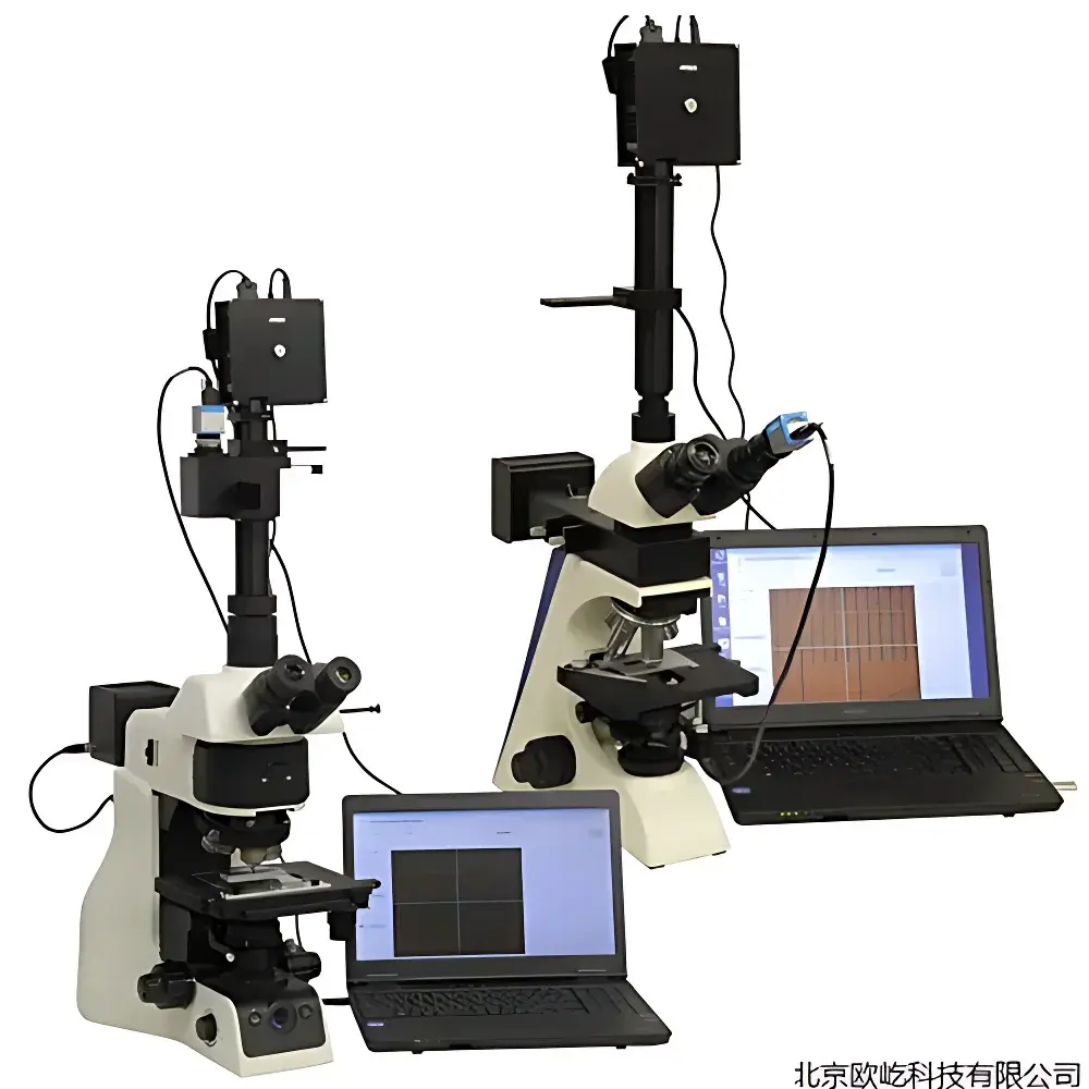
| Optical Architecture | Integrated Metallurgical Microscope + DLP Digital Micromirror Device (DMD) Projection Engine |
| Software-Controlled Pattern Generation | Yes |
| Compatibility | Standalone or Coupled to User-Provided Microscope (Optional Adapter Kit) |
Overview
The ARMS SYSTEM UTA-IA is a compact, projection-based maskless direct-write lithography system engineered for rapid prototyping and low-volume microfabrication in academic research laboratories and semiconductor R&D environments. Unlike conventional photolithography tools requiring physical photomasks, the UTA-IA employs a digital light processing (DLP) engine integrated with a high-precision metallurgical microscope to project user-defined patterns directly onto photoresist-coated substrates. Its optical architecture leverages diffraction-limited visible-light illumination (400–700 nm) from a stabilized LED source, coupled with high-numerical-aperture objectives to achieve consistent 1–2 µm resolution across exposure fields ranging from 100 µm × 100 µm up to 2.5 mm × 1.5 mm. This system operates under ambient laboratory conditions—no vacuum, no electron optics, and no cleanroom-grade infrastructure required—making it significantly more accessible than e-beam lithography while retaining sufficient fidelity for electrode patterning, 2D material device fabrication, and exploratory microstructure definition.
Key Features
- Maskless operation eliminates mask fabrication lead time, cost, and storage constraints.
- DLP-based pattern projection ensures pixel-level control with sub-micron positional repeatability (±0.1 µm typical over repeated exposures).
- Modular optical design allows integration with existing metallurgical microscopes via optional mechanical and optical coupling kits.
- LED illumination provides stable, cold-light output with >10,000-hour lifetime and negligible thermal drift during extended exposure sequences.
- Real-time pattern preview and focus-assisted alignment using on-screen crosshair overlays and live CCD/CMOS camera feed.
- Software supports vector-based (SVG, DXF) and bitmap (BMP, PNG) input formats with layer-aware exposure sequencing and dose calibration per feature group.
Sample Compatibility & Compliance
The UTA-IA accommodates a broad range of substrate geometries and materials—including silicon wafers (up to 4″), glass slides, flexible polymer films, graphene/h-BN flakes on SiO₂/Si, and bulk single-crystal specimens—without requiring vacuum chucking or conductive coating. Substrate flatness tolerance is ±2 µm over the exposure field, compatible with standard spin-coated photoresists (e.g., AZ® series, PMMA, SU-8). The system complies with IEC 61000-6-3 (EMC emission standards) and IEC 60950-1 (safety requirements for electrical equipment). While not certified for ISO Class 5 cleanroom deployment, its enclosed optical path and sealed DMD chamber minimize particulate contamination risk during operation. All exposure parameters—including dwell time, intensity scaling, and multi-pass scanning—are logged with timestamps and operator IDs to support GLP-aligned documentation practices.
Software & Data Management
The proprietary UTA Control Suite runs on Windows 10/11 x64 and provides full GUI-driven workflow management: pattern import/editing, stage coordinate mapping, objective calibration, exposure parameter optimization, and batch job queuing. Each exposure event generates a metadata-rich log file (.xml) containing exposure duration, LED intensity (%), objective magnification, stage position (µm), and checksum-verified pattern hash. Export options include GDSII-compatible layer files (for downstream CAD verification), TIFF-aligned exposure maps, and CSV-formatted process records. Audit trail functionality meets baseline requirements for FDA 21 CFR Part 11 compliance when deployed with network-authenticated user accounts and write-protected log directories.
Applications
- Fabrication of ohmic and Schottky contact electrodes for thin-film transistors (TFTs), Hall bar structures, and nanoribbon devices.
- Patterning of etch masks for transfer printing of 2D materials (graphene, MoS₂, WS₂) without damaging van der Waals interfaces.
- Rapid iteration of interdigitated electrode arrays (IDEs) for electrochemical sensor development.
- Prototyping of plasmonic nanostructures and metamaterial unit cells where sub-5 µm periodicity suffices.
- In-situ lithographic alignment on pre-patterned substrates using fiducial marker recognition algorithms.
FAQ
Does the UTA-IA require a darkroom or vibration isolation table?
No. The system is designed for operation on standard optical tables in ambient lighting; LED-based illumination is insensitive to ambient photons, and mechanical damping is built into the baseplate.
Can grayscale exposure be achieved for tone-controlled development?
Yes—intensity modulation per pixel is supported via 8-bit grayscale mapping, enabling controlled resist dissolution rates for quasi-3D topography.
Is alignment to existing substrate features possible?
Yes, using the integrated camera and manual/semi-automated fiducial registration tools; sub-pixel alignment accuracy of ±0.3 µm is routinely achievable.
What resist thicknesses are compatible with the UTA-IA’s depth-of-field?
Optimal performance is observed with resist films between 0.3 µm and 2.0 µm thick; thicker layers may require multi-pass exposure strategies.
Are maintenance contracts and service-level agreements available?
Yes—ARMS SYSTEM offers annual calibration services, DMD refresh programs, and remote diagnostic support through authorized regional service partners.


