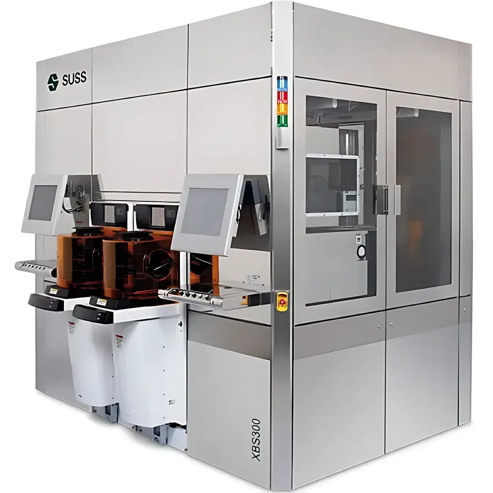
SUSS XBS300 Temporary Bonding Platform
| Brand | SUSS MicroTec |
|---|---|
| Origin | Germany |
| Model | XBS300 |
| Wafer Size | 200 mm / 300 mm |
| Alignment Accuracy (ISA) | < 100 nm |
| Substrate Compatibility | Silicon & Glass Carrier Wafers |
| Modular Configuration | Yes |
| Integrated Metrology | Real-time alignment verification and overlay measurement |
| Process Flexibility | Supports all commercially available temporary bonding adhesives |
| Compliance | Designed for high-volume semiconductor manufacturing environments compliant with ISO 9001, SEMI S2/S8, and compatible with GLP/GMP-aligned process documentation workflows |
Overview
The SUSS XBS300 Temporary Bonding Platform is a production-grade, fully automated system engineered for high-precision temporary bonding of device wafers to carrier substrates in advanced packaging and 3D integration processes. Based on SUSS MicroTec’s proprietary Inter-Substrate Alignment (ISA) technology, the XBS300 delivers sub-100 nm overlay accuracy between bonded layers—critical for fan-out wafer-level packaging (FOWLP), silicon interposer integration, and thin-wafer handling applications. The platform operates on a dual-stage thermal-mechanical bonding principle: precise temperature-controlled chucks (up to 250 °C) apply uniform pressure while maintaining nanoscale positional stability during adhesive activation and consolidation. Its architecture supports both thermoplastic and thermoset temporary bonding materials—including BCB, polyimide-based films, and UV-curable adhesives—enabling seamless transition across front-end and back-end process flows.
Key Features
- Sub-100 nm inter-substrate alignment accuracy enabled by ISA technology, incorporating integrated optical fiducial recognition, global stage calibration, and real-time overlay verification
- Modular platform design supporting field-upgradable configurations: optional vacuum chuck variants, IR heating modules, and inert gas purging for moisture-sensitive adhesives
- Integrated metrology subsystem providing in-situ alignment validation and post-bond thickness uniformity assessment without breaking vacuum or removing wafers
- Dual-wafer handling capability for 200 mm and 300 mm substrates, with automatic edge alignment and notch/orientation detection per SEMI E142 standards
- Thermal management system featuring independent top/bottom chuck control (±0.5 °C uniformity over full surface) and ramp-rate programmability (0.1–10 °C/s)
- Process recipe management with audit-trail logging compliant with FDA 21 CFR Part 11 requirements for electronic records and signatures
Sample Compatibility & Compliance
The XBS300 accommodates standard silicon device wafers (50–775 µm thick) and rigid carrier substrates including fused silica, borosilicate glass (e.g., AF45, Borofloat® 33), and high-resistivity silicon carriers. No recalibration is required when switching between material types due to its adaptive substrate recognition algorithm and multi-point thermal compensation model. All mechanical interfaces conform to SEMI E156 (wafer handling) and E172 (equipment communication protocols). The system meets CE marking requirements under the Machinery Directive 2006/42/EC and Electromagnetic Compatibility Directive 2014/30/EU. Optional IQ/OQ documentation packages support qualification under ISO 14644-1 Class 5 cleanroom environments.
Software & Data Management
Controlled via SUSS’ proprietary BONDmaster™ software suite, the XBS300 provides hierarchical user access levels (Operator, Engineer, Administrator), version-controlled recipe libraries, and automated data export to CSV or SQLite formats. Process logs include timestamped thermal profiles, pressure transducer readings, alignment residuals, and metrology pass/fail flags. Integration with factory MES systems is supported through SECS/GEM (SEMI E30/E37) and OPC UA interfaces. Audit trails record all parameter modifications, user logins, and hardware status events—fully traceable for internal quality audits or external regulatory inspections.
Applications
- Temporary bonding for ultra-thin wafer grinding and polishing (≤ 25 µm final thickness)
- Carrier-assisted lithography and etch processes in hybrid bonding and TSV fabrication
- Reversible bonding in redistribution layer (RDL) formation and microbump patterning
- High-aspect-ratio structure protection during deep reactive ion etching (DRIE)
- Integration into automated tape-and-reel or FOUP-based 300 mm production lines
FAQ
What wafer sizes does the XBS300 support?
The platform handles both 200 mm and 300 mm diameter wafers with automatic size detection and chuck configuration switching.
Is the system qualified for use with UV-curable temporary adhesives?
Yes—the XBS300 offers optional integrated UV exposure modules (365 nm LED array) synchronized with bond force application and temperature ramping.
Can alignment data be exported for statistical process control (SPC)?
All alignment residuals, overlay vectors, and fiducial matching confidence scores are logged and exportable for SPC analysis using standard industry tools.
Does the XBS300 support debonding process integration?
While primarily a bonding platform, it is mechanically and software-compatible with SUSS’ XBR300 debonding systems via shared automation interfaces and recipe synchronization.
How is thermal uniformity validated across the bond chuck?
Each chuck undergoes factory calibration using a 64-point thermocouple grid; real-time uniformity monitoring is performed via embedded Pt100 sensors at eight radial positions.


