EMU Batch Aligner and Elevator for Semiconductor Wafers
| Brand | EMU |
|---|---|
| Origin | United Kingdom |
| Manufacturer Type | Authorized Distributor |
| Origin Category | Imported |
| Model | Batch Aligner and Elevator |
| Wafer Diameters Supported | 75 mm, 100 mm, 125 mm, 150 mm, 200 mm |
| Alignment Reference | Flat or Notch |
| Lifting Mechanism | Dual Non-Vacuum Comb Lifters |
| Illumination | Configurable LED (Standard: Red or White) |
| Substrate Compatibility | Si, SiC, GaN, and Other Compound Semiconductors |
| Interface | Touchscreen HMI with Angle Selection for Edge Alignment |
Overview
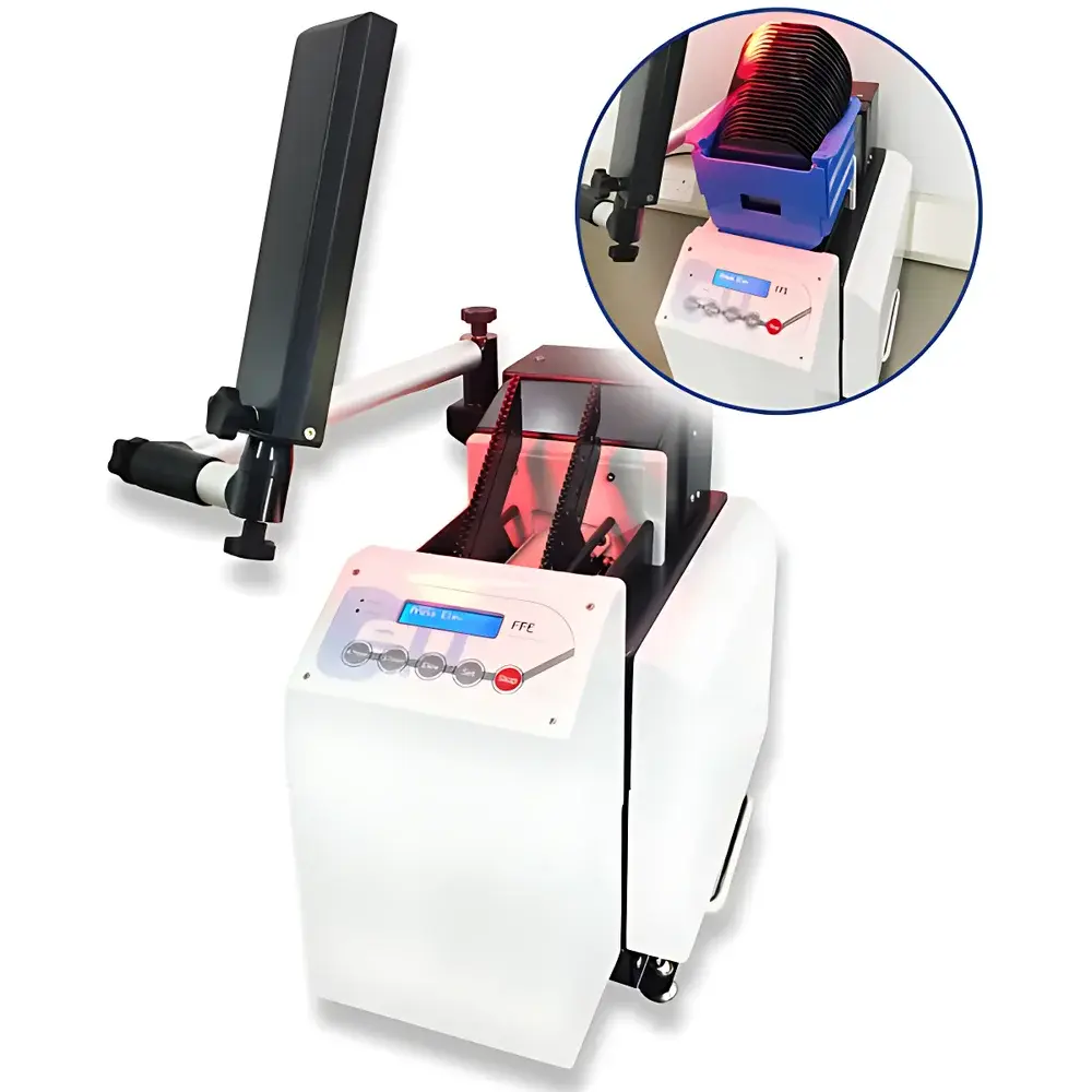
The EMU Batch Aligner and Elevator is a precision-engineered single-station semiconductor handling tool designed to standardize wafer orientation and enable visual inspection prior to downstream processing. It operates on a mechanical alignment principle—leveraging edge detection via optical sensing and physical reference engagement—to achieve repeatable flat- or notch-based alignment across multiple wafers in batch mode. Unlike vacuum-based handlers, this system employs dual non-vacuum comb lifters to elevate wafers from carriers without contact between the aligner platform and either the carrier or wafer surface—minimizing particle generation and mechanical stress. Its robust architecture supports high-reliability operation in cleanroom environments (ISO Class 5 and better), and its modular design allows seamless integration into OEM equipment platforms or standalone IC test and handling workflows.
Key Features
- Batch-mode alignment of up to 25 wafers per cycle (dependent on carrier type and diameter)
- Programmable alignment angle selection via intuitive touchscreen HMI—enabling precise rotational registration relative to flat or notch features
- Non-contact lifting mechanism using dual stainless-steel comb lifters; eliminates vacuum lines, residual suction, and associated contamination risks
- Integrated LED illumination module with configurable wavelength output (standard red or white; optional blue or UV variants available upon request) for enhanced edge contrast during manual or machine vision inspection
- Passive thermal stability design—no active cooling or heating required—ensuring dimensional consistency across ambient temperature fluctuations (18–25 °C)
- Modular mounting interface compatible with standard SEMI E19.01 carrier footprints and FOUP/SMIF load ports
Sample Compatibility & Compliance
The aligner accommodates bare and coated wafers across five standard diameters: 75 mm, 100 mm, 125 mm, 150 mm, and 200 mm. It is validated for use with silicon (Si), silicon carbide (SiC), gallium nitride (GaN), sapphire, and other compound semiconductor substrates—including those with fragile epitaxial layers or low-dielectric thin films. All mechanical interfaces comply with SEMI Standard E19.01 (Mechanical Interface for 200 mm FOUPs) and E47.1 (Load Port Interface Specifications). The system meets CE marking requirements under the Machinery Directive 2006/42/EC and Electromagnetic Compatibility Directive 2014/30/EU. Optional documentation packages support GLP/GMP audit readiness, including IQ/OQ protocols aligned with ISO 9001:2015 and ISO 13485:2016 frameworks.
Software & Data Management
The embedded control firmware runs on a real-time Linux kernel with deterministic I/O response (<10 ms latency). Alignment parameters—including selected reference edge (flat/notch), rotation offset, illumination intensity, and lift height—are stored per recipe and recalled via alphanumeric naming. Audit trails record all operator actions, parameter changes, and system status transitions with timestamps traceable to UTC. Optional Ethernet/IP or SECS/GEM connectivity enables integration into factory automation systems (MES/SCADA) and supports data export in CSV or XML format. Firmware updates are performed via secure USB key with SHA-256 signature verification—fully compliant with FDA 21 CFR Part 11 requirements for electronic records and signatures when deployed in regulated manufacturing environments.
Applications
- Pre-probe alignment in wafer-level testing stations to ensure consistent chuck placement and probe card registration
- Post-lithography or post-etch visual QA inspection of pattern fidelity, edge chipping, and bevel defects
- OEM integration into automated die sorters, laser trim systems, and AOI platforms requiring deterministic wafer orientation
- R&D lab environments handling prototype SiC and GaN power devices where electrostatic discharge (ESD) sensitivity precludes vacuum handling
- Education and training setups for semiconductor process engineering courses emphasizing mechanical handling fundamentals
FAQ
Does the aligner support automatic vision-based alignment?
No—it performs mechanical edge referencing only. Vision-based alignment requires integration with an external camera system and third-party image processing software.
Can it handle warped or bowed wafers?
Yes—within industry-standard warp limits (≤30 µm for 200 mm Si wafers per SEMI MF-1530); the comb lifters engage only at the outermost 3 mm of the wafer edge, minimizing distortion transfer.
Is calibration required before each run?
No—factory calibration is retained across power cycles. Annual verification using NIST-traceable alignment gauges is recommended per ISO/IEC 17025 guidelines.
What maintenance intervals apply?
Lifter comb wear inspection every 10,000 cycles; LED illumination output verification every 6 months; HMI touchscreen calibration as needed—documented in the included Preventive Maintenance Logbook.
Is the system compatible with 300 mm wafers?
Not natively—the current platform is engineered for ≤200 mm substrates. A 300 mm variant is under development and scheduled for release in Q4 2025.


