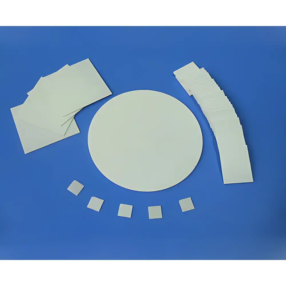
Al2O3 Ceramic Substrate (96%–99.6% Purity), Hefei Kejing Model
| Brand | Hefei Kejing |
|---|---|
| Origin | Anhui, China |
| Manufacturer Type | Authorized Distributor |
| Origin Category | Domestic |
| Model | Al2O3 Ceramic Substrate |
| Price | Upon Request |
| Purity (wt%) | 96–99.6 |
| Density (g/cm³) | >3.75 |
| Thermal Conductivity (W/m·K) | 24 |
| CTE (×10⁻⁶/°C) | <7.7 |
| Dielectric Strength (kV/mm) | >14 |
| Dielectric Constant (at 1 MHz) | 9.8 |
| Loss Tangent (×10⁻⁴ @ 1 MHz) | 4 |
| Flexural Strength (MPa) | >330 |
| Volume Resistivity (Ω·m) | >10¹³ @ 20°C, >3×10⁷ @ 500°C |
| Surface Roughness (Ra) | <0.8 nm |
| Dimensions | 2″×2″×0.5 mm |
| Packaging | Class 1000 cleanroom assembled |
Overview
Al2O3 ceramic substrates are high-performance insulating platforms engineered for demanding electronic, thermal management, and vacuum-compatible applications. Composed of sintered aluminum oxide with controlled stoichiometry and microstructure, these substrates operate on the principle of structural stability under thermal cycling, electrical isolation at high voltages, and efficient lateral heat dissipation via phonon conduction. With purity levels ranging from 96% to 99.6% (wt%), they balance cost-effectiveness with critical functional attributes—particularly where hermetic sealing, low outgassing, and dimensional stability across -55°C to +850°C are required. The material’s hexagonal corundum crystal lattice provides intrinsic resistance to chemical corrosion, plasma erosion, and ion implantation, making it suitable for semiconductor packaging, power module mounting, MEMS sensor carriers, and high-temperature furnace linings.
Key Features
- Controlled purity grades (96%, 99.5%, and 99.6% Al2O3) enabling selection based on dielectric integrity vs. thermal budget requirements
- Density exceeding 3.75 g/cm³ ensures minimal porosity (<0.5% vol.) and high mechanical rigidity
- Thermal conductivity of 24 W/m·K supports effective heat spreading in high-power LED assemblies and RF amplifier modules
- Coefficient of thermal expansion (CTE) below 7.7 × 10⁻⁶/°C enables reliable co-firing and bonding with common metallization systems (e.g., Mo/Mn, W, Ag-Pd)
- Dielectric strength >14 kV/mm and volume resistivity >10¹³ Ω·m at room temperature ensure robust insulation in high-voltage DC-link applications
- Fine-ground surface finish (Ra < 0.8 nm) facilitates uniform thin-film deposition, precise wire bonding alignment, and low-contact-resistance soldering
- Customizable geometry—including non-standard aspect ratios, chamfered edges, and laser-drilled vias—supports application-specific integration into hybrid circuits and microsystems
Sample Compatibility & Compliance
These substrates comply with industry-standard material qualification protocols for electronic ceramics, including ASTM C20 (bulk density and apparent porosity), ASTM C1161 (flexural strength), and IEC 60672-3 (ceramic classification). They meet RoHS Directive 2011/65/EU for restricted substances and exhibit ultra-low outgassing rates (<1×10⁻⁹ Torr·L/s·cm² at 120°C), qualifying them for UHV environments per NASA SP-R-0022A. Batch traceability is maintained through lot-controlled sintering records, and each shipment includes a Certificate of Conformance listing measured CTE, dielectric constant, and surface roughness. For medical device or aerospace use, optional ISO 9001:2015-certified manufacturing documentation and particulate testing (per ISO 14644-1 Class 5) are available upon request.
Software & Data Management
While Al2O3 substrates are passive components, their integration into automated production workflows benefits from standardized data exchange formats. Hefei Kejing provides substrate specifications in SPICE-compatible thermal network models (.lib), IPC-2581-compliant fabrication data packages, and STEP AP210 files for mechanical CAD integration. Traceability metadata—including sintering batch ID, grain size distribution histograms (from SEM cross-section analysis), and post-grinding surface topography maps (via white-light interferometry)—are archived in secure, audit-ready digital dossiers aligned with ISO/IEC 17025 requirements for calibration laboratories. All documentation supports GLP/GMP-compliant record retention for regulated industries.
Applications
- Power electronics: Baseplates and isolation layers in IGBT modules, SiC MOSFET packages, and EV traction inverters
- Sensors & actuators: Carrier substrates for piezoresistive pressure sensors, pyroelectric IR detectors, and high-temperature strain gauges
- Optoelectronics: Mounting platforms for laser diodes, VCSEL arrays, and photonic integrated circuit (PIC) housings
- Vacuum & plasma systems: Feedthrough insulators, electrode supports, and chamber liners in PVD/CVD tools and fusion diagnostics
- Research infrastructure: Sample holders for in-situ TEM heating stages, synchrotron XRD sample cells, and cryogenic quantum device test fixtures
FAQ
What is the maximum operating temperature for these Al2O3 substrates?
Continuous operation is rated up to 850°C in air; short-term exposure to 1600°C is permissible under inert atmospheres without structural degradation.
Can these substrates be metallized using standard thick-film or thin-film processes?
Yes—they are fully compatible with Mo-Mn metallization (for glass-sealable packages), sputtered TiW/Cu stacks, and electroless Ni-P plating, provided surface cleanliness (measured by water contact angle <5°) is verified prior to processing.
Is surface roughness guaranteed per batch, and how is it verified?
Each lot undergoes non-contact optical profilometry (Zygo NewView 9000) at five locations per substrate; Ra values are reported in the CoC with ±0.05 nm uncertainty (k=2).
Do you offer hermetic sealing validation data for bonded assemblies?
Yes—helium leak rate data (<1×10⁻⁸ std cm³/s) and thermal shock performance (500 cycles between -40°C and +150°C) are available for common Al2O3/Kovar and Al2O3/Cu composite structures.
Related Products
 and Vehicle Classification System")