Al2O3 Sapphire Crystal Substrates – Hefei Kejing Model Al2-O-3 for QCM and Thin-Film Epitaxy
| Brand | Hefei Kejing |
|---|---|
| Origin | Anhui, China |
| Model | Al2-O-3 |
| Crystal Structure | Hexagonal (α-Al₂O₃) |
| Lattice Constants | a = 4.758 Å, c = 12.992 Å |
| Orientations Available | c-plane (0001), a-plane (11–20), m-plane (10–10), r-plane (1–102) |
| Purity | >99.99% |
| Melting Point | 2040 °C |
| Density | 3.98 g/cm³ |
| Mohs Hardness | 9 |
| Thermal Expansion Coefficient | 7.5 × 10⁻⁶ /°C |
| Thermal Conductivity | 46.06 W/(m·K) @ 0 °C, 25.12 W/(m·K) @ 100 °C, 12.56 W/(m·K) @ 400 °C |
| Dielectric Constant | εₐ ≈ 9.4 @ 300 K, ε꜀ ≈ 11.58 @ 300 K |
| Loss Tangent | tan δ < 2 × 10⁻⁵ (a-axis), < 5 × 10⁻⁵ (c-axis) |
| Surface Finish | Single- or double-side polished, Ra < 0.5 nm |
| Orientation Tolerance | ±0.2° |
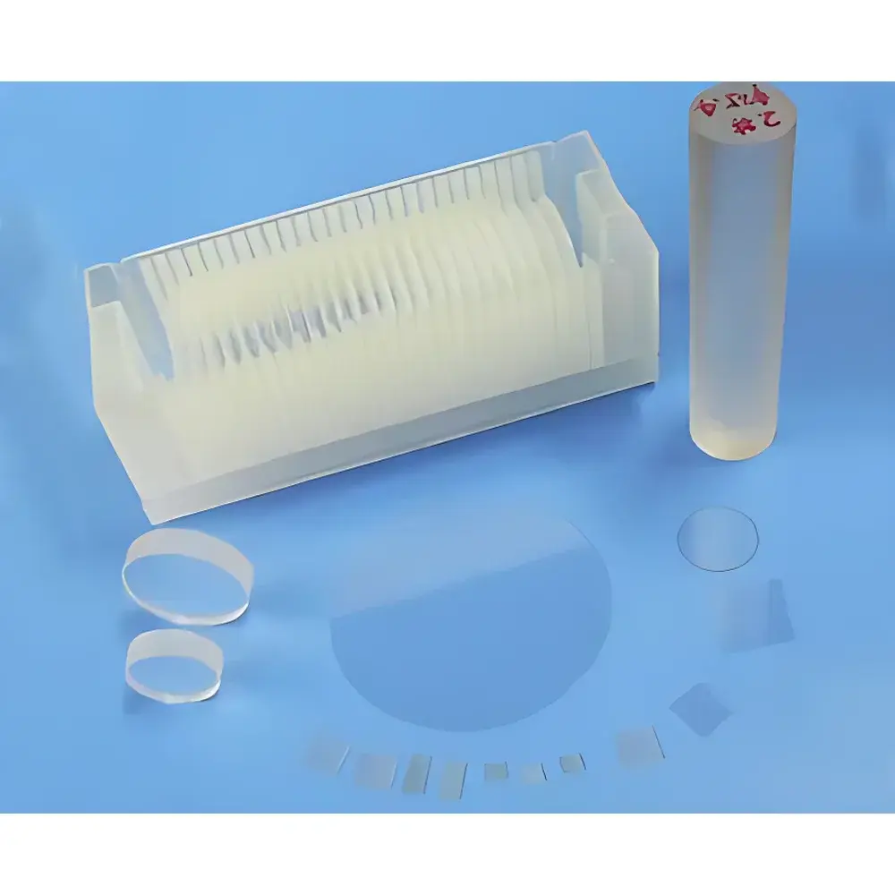
| Standard Dimensions | Ø76.2 mm × 0.5 mm, Ø50.8 mm × 0.5 mm, 10 × 10 × 0.5 mm³, 10 × 5 × 0.5 mm³ |
| Packaging | Class 1000 cleanroom processed, sealed in Class 100 clean bags or individual substrate carriers |
Overview
Hefei Kejing Al2O3 Sapphire Crystal Substrates (Model Al2-O-3) are high-purity, single-crystal aluminum oxide wafers engineered for demanding applications in quartz crystal microbalance (QCM) sensing, epitaxial thin-film growth, optical window fabrication, and high-frequency electronic device platforms. As a member of the corundum family, α-Al2O3 exhibits exceptional thermal stability, wide bandgap (~9.9 eV), low dielectric loss, and atomic-level surface regularity—making it a foundational platform for III-nitride (e.g., GaN, AlN) and ZnO heteroepitaxy, as well as mass-sensitive biosensing and electrochemical interface studies using QCM-D configurations. Its hexagonal crystal symmetry, defined by lattice parameters a = 4.758 Å and c = 12.992 Å, enables precise orientation control across four industrially relevant crystallographic planes: c-plane (0001), a-plane (11–20), m-plane (10–10), and r-plane (1–102). Each wafer is grown via the Kyropoulos or Czochralski method, followed by precision lapping, double-side polishing (Ra < 0.5 nm), and rigorous metrological verification to ensure angular tolerance within ±0.2°.
Key Features
- Ultra-high purity (>99.99% Al2O3) with trace metal impurities controlled below detection limits per ICP-MS analysis
- Thermally stable up to 2040 °C; coefficient of thermal expansion (7.5 × 10⁻⁶ /°C) compatible with GaN and SiC layer integration
- Exceptional mechanical robustness (Mohs hardness = 9) enabling durable handling in vacuum deposition, plasma etching, and sputtering environments
- Low dielectric loss (tan δ < 2 × 10⁻⁵ on a-axis; < 5 × 10⁻⁵ on c-axis) critical for RF-MEMS and GHz-range resonator substrates
- Optical transparency from deep UV (190 nm) through mid-infrared (5.5 µm), validated for IR window and laser host applications
- Controlled surface roughness (Ra < 0.5 nm) verified by AFM and optical interferometry; available in single- or double-side polished configurations
- Customizable crystallographic orientation, thickness (standard 0.5 mm; optional 0.3–1.0 mm), and geometry (round, square, rectangular)
Sample Compatibility & Compliance
These substrates are routinely employed in ISO/IEC 17025-accredited laboratories for calibration-grade QCM sensor development and as seed layers in MOCVD and MBE systems compliant with SEMI F47 and ASTM F1523 standards. Their chemical inertness ensures compatibility with aggressive etchants (e.g., hot phosphoric acid for GaN lift-off), reactive plasmas (CF4/O2, Cl2/BCl3), and high-temperature annealing (>1000 °C) under N2, O2, or forming gas atmospheres. All wafers undergo final inspection in ISO Class 5 (100) cleanroom conditions and are packaged in static-dissipative, particle-controlled containers meeting IPC-CC-830B requirements for electronic substrate storage.
Software & Data Management
While inherently passive components, these substrates integrate seamlessly into automated thin-film deposition platforms (e.g., Veeco GEN10, Oxford Instruments PlasmaLab) and QCM instrumentation (e.g., Biolin QSense, SRS SR780) that support GLP-compliant data logging, audit trails, and instrument qualification records per FDA 21 CFR Part 11. Traceability includes lot-specific certificates of conformance detailing XRD rocking curve FWHM (< 30 arcsec for c-plane), surface defect density ( 0.3 µm), and orientation verification reports.
Applications
- Epitaxial template for GaN-based LEDs, laser diodes (LDs), and high-electron-mobility transistors (HEMTs)
- Substrate for piezoelectric AlN and ScAlN thin-film resonators (TFMRs) and BAW filters
- Active sensing platform in liquid-phase QCM biosensors for real-time protein adsorption, cell adhesion, and polymer film swelling kinetics
- Inert support for electrochemical impedance spectroscopy (EIS) and cyclic voltammetry in corrosive electrolytes
- IR-transmissive window material for FTIR spectrometers, CO2 lasers, and high-temperature furnace viewports
- Reference standard for Raman spectroscopy calibration and XRD texture analysis
FAQ
What crystal orientations are available, and how is orientation accuracy verified?
Standard options include c-plane (0001), a-plane (11–20), m-plane (10–10), and r-plane (1–102), each confirmed by high-resolution X-ray diffraction (HR-XRD) with angular tolerance ±0.2° relative to the nominal Miller index.
Can these substrates be used directly in ultra-high vacuum (UHV) systems without outgassing concerns?
Yes—fully degassed at 400 °C in vacuum prior to packaging; total hydrocarbon contamination < 1 ng/cm² per ESCA verification; suitable for UHV MBE and ALD processes.
Is double-side polishing necessary for QCM applications?
For fundamental-mode 5–10 MHz QCM devices, single-side polish suffices; however, double-side polish (Ra 25 MHz) resonators to minimize acoustic energy dissipation.
Do you provide documentation supporting ISO 13485 or GMP manufacturing practices?
While not medical-device-manufactured, production follows documented cleanroom protocols aligned with ISO 14644-1 Class 5 environments and includes full traceability records compatible with GMP Annex 11 and EU GMP Chapter 4 quality system requirements.
Are custom thicknesses or non-standard geometries supported?
Yes—custom thicknesses from 0.3 mm to 1.0 mm, rectangular dimensions up to 50 × 50 mm, and chamfered or beveled edge options are available upon engineering review and minimum order quantity agreement.