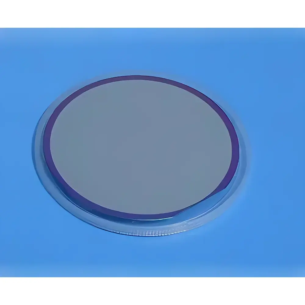
Al2O3/ZnO Heteroepitaxial Thin-Film Substrate on Sapphire (C-plane)
| Brand | MTI Corporation |
|---|---|
| Origin | USA |
| Manufacturer Type | Authorized Distributor |
| Origin Category | Imported |
| Model | Al₂O₃/ZnO |
| Thickness | 500 Å (0.5 µm) ±5% |
| Crystal Orientation | c-plane (0001) |
| Resistivity | 10–10³ Ω·cm |
| Surface Finish | Single-side polished |
| Standard Diameter × Thickness | 50.8 mm × 0.5 mm |
| Packaging | Vacuum-sealed in Class 100 cleanroom bags inside Class 1000 cleanroom environment, or individual wafer cassette |
Overview
The Al₂O₃/ZnO heteroepitaxial thin-film substrate is a high-purity, lattice-matched semiconductor-on-insulator platform engineered for advanced optoelectronic and wide-bandgap device research. Fabricated via metal-organic chemical vapor deposition (MOCVD) or pulsed laser deposition (PLD), this structure consists of a ZnO epitaxial layer grown on single-crystal sapphire (Al₂O₃) with precise orientation. The c-plane sapphire substrate provides exceptional thermal stability, low dielectric loss, and minimal lattice mismatch (~1.3%) with wurtzite ZnO—enabling high-crystallinity, low-defect-density films essential for UV photodetectors, transparent thin-film transistors (TFTs), piezoelectric sensors, and heterojunction light-emitting diodes (LEDs).
Key Features
- Epitaxial ZnO layer with controlled stoichiometry and low oxygen vacancy concentration, verified by XRD rocking curve FWHM ≤ 0.2°
- Atomically smooth surface (RMS roughness < 0.3 nm over 5×5 µm AFM scan) enabling uniform ALD and sputtering nucleation
- Thermally stable up to 1000 °C in inert atmosphere—compatible with high-temperature post-deposition annealing protocols
- Optical transparency >85% in the visible range (400–700 nm) and strong near-UV absorption edge at ~370 nm
- Consistent thickness control within ±5% across full wafer area, certified via spectroscopic ellipsometry and cross-sectional TEM
- Single-side polished finish meeting SEMI standard SF1 for optical and electron-beam lithography alignment
Sample Compatibility & Compliance
This substrate is compatible with standard semiconductor fabrication workflows including photolithography (i-line, KrF, and e-beam), reactive ion etching (RIE) using CH₄/H₂ or BCl₃-based chemistries, and metallization (Ti/Al/Ni/Au, Cr/Au). It conforms to ISO 14644-1 Class 5 (ISO Class 5 / Fed Std 209E Class 100) cleanroom handling requirements. All wafers undergo pre-shipment inspection per ASTM F1529-21 (Standard Practice for Visual Inspection of Silicon Wafers) adapted for compound substrates. Traceable documentation includes crystallographic orientation verification report, surface roughness map, and resistivity certificate measured using four-point probe per ASTM F84-22.
Software & Data Management
While the substrate itself is a passive material platform, its metrological traceability supports integration into GLP- and GMP-compliant R&D environments. Batch-specific certificates of analysis (CoA) include unique lot numbers, deposition date, and QA test records stored in secure cloud archives compliant with FDA 21 CFR Part 11 for electronic records and signatures. Users may import substrate metadata—including thickness, orientation, and resistivity—into laboratory information management systems (LIMS) or MES platforms via standardized CSV or JSON export templates provided upon request.
Applications
- Development of high-responsivity, solar-blind UV photodetectors operating below 280 nm
- Fabrication of normally-off ZnO-based power transistors leveraging Al₂O₃’s high-k dielectric properties (κ ≈ 9)
- Model system for studying interfacial polarization, piezotronic effects, and strain-mediated ferroelectric coupling at oxide heterojunctions
- Template for subsequent growth of GaN, MgZnO, or graphene layers via van der Waals epitaxy
- Calibration reference for in-situ ellipsometry, reflectance anisotropy spectroscopy (RAS), and surface photovoltage measurements
FAQ
Is this substrate suitable for atomic layer deposition (ALD) of high-k gate oxides?
Yes—the atomically ordered ZnO surface and native hydroxyl termination provide ideal nucleation sites for Al₂O₃, HfO₂, and ZrO₂ ALD processes.
What is the typical threading dislocation density (TDD) in the ZnO layer?
Typical TDD ranges from 1×10⁸ to 5×10⁸ cm⁻², as confirmed by plan-view TEM and cathodoluminescence mapping.
Can I order custom diameters or thicknesses?
Custom geometries (e.g., 76.2 mm diameter, double-side polished, or 1.0 mm substrate thickness) are available under NRE-supported engineering lots with minimum order quantities.
Do you provide wafer-level electrical characterization data?
Four-point probe sheet resistance maps and Hall effect mobility data (at 300 K and 77 K) are included in optional extended CoA packages.
How is contamination controlled during packaging?
Each wafer is handled in ISO Class 5 laminar flow hoods, inspected under 200× dark-field microscopy, and sealed in nitrogen-purged, static-dissipative Class 100 bags with humidity indicators.