Auniontech RTM2 Hall Effect Source-Measure Unit (SMU) System
| Brand | Auniontech |
|---|---|
| Origin | Shanghai, China |
| Manufacturer Type | Authorized Distributor |
| Product Category | Domestic |
| Model | Current Source-Measure Unit |
| Pricing | Available Upon Request |
Overview
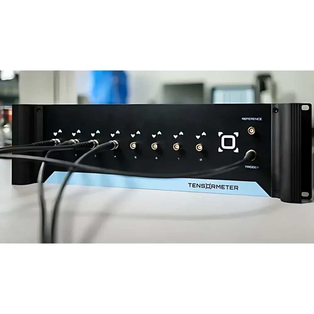
The Auniontech RTM2 Hall Effect Source-Measure Unit (SMU) System is a precision electrical characterization platform engineered for high-fidelity, low-noise DC and AC resistance metrology in semiconductor and advanced material research. Unlike conventional four-terminal (Kelvin) or static SMU-based approaches, the RTM2 implements a fully reconfigurable 8-port matrix switching architecture that enables time-domain separation of systematic errors—including thermoelectric offsets, contact potential drifts, and amplifier gain instability—thereby achieving metrological-grade stability over extended measurement durations. Its core operation leverages the van der Pauw method and full resistivity tensor extraction without requiring lithographically defined geometries, making it uniquely suited for characterizing as-grown thin films, irregular substrates, and emerging 2D materials. The system integrates source, measure, and switching functions into a single instrument, eliminating inter-device synchronization latency and cabling-induced noise coupling. It operates on fundamental principles of low-frequency lock-in amplification (with built-in reference demodulation), ultra-stable current sourcing (1 TΩ with reproducibility at the ppb level.
Key Features
- 8 independently configurable BNC ports supporting user-defined input/output/reference roles per channel
- Passive grounding or active guarding capability for each port to suppress leakage currents and extend DC impedance range beyond 1 TΩ
- Integrated matrix switch enabling automated, sequential 4-wire connections for van der Pauw, Hall geometry, and resistivity tensor (Rx, Ry, RH) acquisition
- Simultaneous dual-channel AC/DC excitation and measurement with phase-sensitive detection (0.001–10 kHz bandwidth)
- Auto-zeroing and gain-drift compensation algorithms implemented in firmware—achieving effective resolution beyond 8½ digits given sufficient averaging time
- TCP/IP-based SCPI command interface compatible with LabVIEW, Python (PyVISA), MATLAB, and C/C++ environments
- Preset measurement sequences for standard protocols including zero-field Hall, offset-compensated transverse resistance, and harmonic distortion analysis up to 5th order
Sample Compatibility & Compliance
The RTM2 supports direct interfacing with probe stations (manual and semi-automated), cryogenic dewars (4 K to 300 K), vacuum chambers (<10−6 mbar), and environmental test enclosures. Its open-architecture design accommodates non-patterned samples—such as sputtered oxide films, exfoliated TMD monolayers, organic semiconductors, and topological insulator flakes—without lithographic processing. From a regulatory standpoint, the system’s deterministic switching sequence, timestamped data logging, and full audit trail support GLP-compliant workflows. While not pre-certified to ISO/IEC 17025, its traceable calibration methodology aligns with ASTM F1995 (Standard Test Method for Sheet Resistance of Semiconductor Wafers Using the Van Der Pauw Technique) and IEC 60404-5 (Magnetic Materials – Part 5: Magnetic Properties of Permanent Magnet Materials). Firmware logs include full metadata (temperature, bias history, switching state, integration time), satisfying basic FDA 21 CFR Part 11 requirements for electronic records when deployed in regulated R&D settings.
Software & Data Management
The RTM2 ships with cross-platform control software (Windows/macOS/Linux) providing intuitive graphical configuration of switching matrices, excitation waveforms (DC, sine, square, pulsed), and demodulation parameters. All raw and processed data are stored in HDF5 format—supporting hierarchical metadata embedding, lossless compression, and programmatic access via Python h5py or MATLAB h5read. The software includes built-in routines for temperature-dependent resistivity mapping, carrier concentration/mobility extraction (via multi-field Hall analysis), and nonlinear I-V curve fitting using Levenberg-Marquardt optimization. Export options include CSV, MATLAB .mat, and standardized JSON-LD for LIMS integration. Remote operation is supported via TCP socket with full SCPI command set compliance; no proprietary drivers are required.
Applications
- Van der Pauw and Hall effect characterization of unpatterned epitaxial layers (e.g., GaN, SiC, perovskites)
- Resistivity tensor mapping in anisotropic crystals (e.g., black phosphorus, ReS2) and heterostructures
- Sub-ppm nonlinearity analysis for identifying higher-order transport mechanisms (e.g., Mott variable-range hopping, bipolaron conduction)
- In-situ process monitoring during atomic layer deposition (ALD) or molecular beam epitaxy (MBE)
- Quality assurance testing of transparent conductive oxides (TCOs) and flexible electrode stacks
- Fundamental studies of quantum oscillations, weak localization, and spin-momentum locking in topological materials
- High-reliability screening of memory devices (RRAM, MRAM) under thermal stress and bias cycling
FAQ
Does the RTM2 require external lock-in amplifiers or SMUs?
No—the RTM2 integrates all necessary signal generation, conditioning, and demodulation circuitry internally. External instruments are neither required nor recommended for standard operation.
Can the RTM2 perform pulsed I-V measurements?
Yes—it supports user-defined current/voltage pulse trains with programmable rise/fall times (≥10 µs), dwell periods, and trigger synchronization via TTL inputs.
Is calibration traceable to national standards?
Calibration is performed using NIST-traceable shunt resistors and voltage references; full calibration certificates with uncertainty budgets are available upon request.
What sample mounting configurations are supported?
Standard configurations include 4-point probe, Hall bar (with optional magnetic field alignment jigs), and arbitrary electrode placement on planar substrates—no photolithography needed.
How is thermal EMF minimized during low-resistance measurements?
The system employs copper-to-copper connections, thermally symmetric PCB layout, and real-time offset subtraction using alternating polarity current sweeps—reducing thermal EMF contribution to <10 nV.
Related Products


 for EMI Conducted Emission & Immunity Testing")