Axetris FAC/SAC Series Micro-Optical Lenses
| Brand | Axetris |
|---|---|
| Origin | Switzerland |
| Product Type | Micro-Optical Components |
| Material | Silicon & Fused Silica |
| Wavelength Range | UV to Mid-IR |
| Lens Types | Aspheric Microlenses & Microlens Arrays |
| Primary Applications | Fiber Coupling, LD/VCSEL Collimation, Optical Sensing, Telecom Systems |
| Compliance | Telcordia GR-1209-CORE, GR-1221-CORE |
| OEM Support | Full Design-to-Volume Manufacturing Services |
Overview
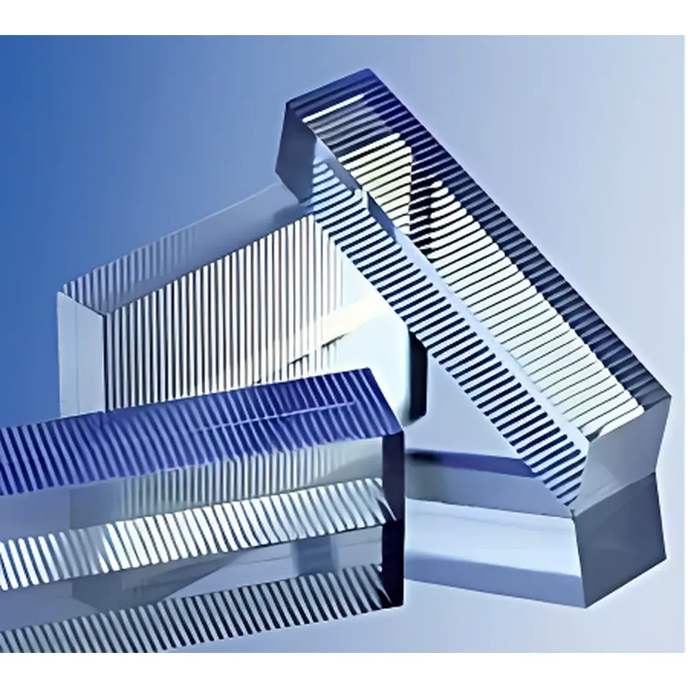
Axetris FAC (Fast Axis Collimation) and SAC (Slow Axis Collimation) series micro-optical lenses are precision-engineered monolithic microlenses and microlens arrays fabricated from single-crystal silicon and fused silica. These components operate on refractive optical principles and are optimized for high-fidelity beam shaping in demanding photonic systems. Designed for integration into compact optomechanical assemblies, they enable diffraction-limited performance across a broad spectral range—from 193 nm (deep UV) to 4.5 µm (mid-infrared)—without thermal or mechanical hysteresis. Their monolithic construction eliminates adhesive-induced degradation, ensuring long-term stability under thermal cycling and high-power irradiation. Axetris leverages deep reactive ion etching (DRIE) and precision diamond turning to achieve sub-50 nm surface roughness and radius-of-curvature (ROC) uniformity better than ±0.5%, critical for minimizing wavefront error in single-mode fiber coupling and laser diode collimation.
Key Features
- Monolithic fabrication in silicon (for IR applications) and fused silica (for UV–VIS–NIR transmission)
- Aspheric surface profiles engineered to eliminate spherical aberration in fast-axis and slow-axis collimation of edge-emitting LDs and VCSELs
- Array pitch tolerance ≤ ±0.3 µm; ROC uniformity < ±0.5% across full array (e.g., 1×8, 1×12, 2×4 configurations)
- Insertion loss < 0.3 dB per channel in single-mode fiber array coupling (SMF-28, 125 µm cladding)
- Telcordia GR-1209-CORE and GR-1221-CORE qualified for reliability in telecom-grade modules
- OEM-customizable parameters: numerical aperture (NA up to 0.65), working distance (100 µm to 2 mm), focal length (100 µm to 1.5 mm), and substrate thickness (0.3–1.0 mm)
Sample Compatibility & Compliance
These micro-optical components are compatible with standard semiconductor packaging processes—including flip-chip bonding, active alignment under interferometric feedback, and hermetic sealing in TO-can and butterfly housings. They support industry-standard fiber array substrates (e.g., V-groove silicon wafers with 127 µm or 250 µm pitch) and integrate seamlessly with InP-based laser sources, Si photonics transceivers, and MEMS-based wavelength-selective switches. All FAC/SAC lenses comply with ISO 10110-7 for surface imperfections and ISO 9022-3 for environmental robustness. For regulated medical and aerospace applications, documentation packages include traceable metrology reports (Zygo Verifire Interferometer), material certificates (RoHS/REACH), and process control records aligned with ISO 9001:2015 and IATF 16949.
Software & Data Management
While the lenses themselves are passive optical elements, Axetris provides comprehensive optical design support files—including Zemax-compatible .ZAR and Code V .SEQ files—for each standard FAC/SAC configuration. These models incorporate measured surface figure data, coating specifications (e.g., MgF₂ AR at 1550 nm or broadband 400–1700 nm), and thermal expansion coefficients. For volume OEM customers, Axetris delivers statistical process control (SPC) dashboards covering lens height, ROC, and centration error across wafer lots. All manufacturing data is archived for ≥15 years and supports audit readiness for FDA 21 CFR Part 11 (when integrated into Class II medical laser systems) and GLP/GMP traceability requirements.
Applications
- Single-mode fiber array coupling in CFP2/OSFP transceivers and co-packaged optics
- Collimation of high-power 9xx nm pump diodes and 850 nm VCSEL arrays in datacom transmitters
- Beam homogenization in structured-light 3D sensing modules (e.g., facial recognition, LiDAR illumination)
- Input/output coupling in planar lightwave circuit (PLC) splitters and arrayed waveguide gratings (AWGs)
- Optical path conditioning in portable FTIR spectrometers and tunable diode laser absorption spectroscopy (TDLAS) gas analyzers
- Free-space interconnects in quantum computing cryogenic optical interfaces
FAQ
What is the maximum power density these lenses can withstand without damage?
Silicon-based FAC lenses are rated for continuous-wave operation up to 5 kW/cm² at 1064 nm; fused silica variants support >10 J/cm² for nanosecond pulsed lasers (10 ns, 10 Hz) at 355 nm.
Can Axetris provide anti-reflection coatings optimized for custom wavelength bands?
Yes—custom dielectric stacks (e.g., Ta₂O₅/SiO₂) are available for narrowband (±2 nm) or broadband (400–2000 nm) AR performance, with residual reflectivity < 0.2% per surface.
Is wafer-level testing performed on every production lot?
Yes—100% interferometric verification (phase-shifting interferometry) and automated centroid alignment metrology are conducted per wafer, with full SPC reporting per ISO 22514-2.
Do FAC/SAC lenses support active alignment during module assembly?
All standard designs include fiducial marks (laser-etched crosshairs) and reference flats enabling sub-micron active alignment using vision-based or interferometric positioning systems.
What is the lead time for custom-designed microlens arrays?
Typical NRE cycle is 8–10 weeks for first-article delivery, including mask fabrication, DRIE process qualification, and metrology validation; volume production ramp begins at week 12 post-design freeze.


