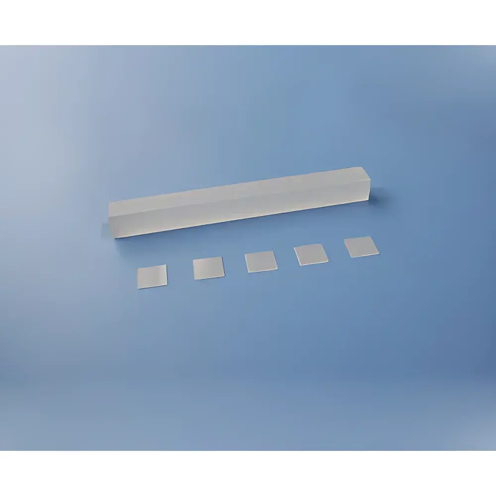
BGO Crystal Substrates (Bi₄Ge₃O₁₂)
| Brand | Hefei Kejing |
|---|---|
| Origin | Anhui, China |
| Manufacturer Type | Authorized Distributor |
| Origin Category | Domestic |
| Model | BGO Crystal Substrates |
| Pricing | Upon Request |
| Crystal Orientation | <100> |
| Crystal Structure | Cubic |
| Lattice Constant | a = 10.518 Å |
| Growth Method | Czochralski (Cz) |
| Melting Point | 1050 °C |
| Density | 7.12 g/cm³ |
| Mohs Hardness | 5 |
| Transmission Range | 350–5500 nm |
| Electro-Optic Coefficient r₄₁ | 1.03 × 10⁻¹² m/V |
| Refractive Index | 2.098 @ 632.8 nm |
| Excitation Peak | 305 nm |
| Emission Spectrum | 480–510 nm |
| Relative Light Output | 10–14% vs. NaI(Tl) |
| Decay Time | 300 ns |
| Critical Energy | 10.5 MeV |
| Energy Resolution @ 511 keV | 20% |
| Packaging | Class 1000 cleanroom environment |
Overview
BGO Crystal Substrates (Bi4Ge3O12) are high-purity, optically transparent single-crystal wafers engineered for use as scintillation detector elements in radiation detection and measurement systems. As a cubic oxide scintillator with no intrinsic birefringence, BGO exhibits strong stopping power for high-energy photons and charged particles due to its high effective atomic number (Zeff ≈ 74) and density (7.12 g/cm³). Its primary luminescence mechanism is based on radiative recombination within the crystal lattice following ionization by incident X-ray or γ-ray photons. The characteristic emission peak at 480 nm—within the spectral sensitivity range of standard photomultiplier tubes (PMTs) and silicon photomultipliers (SiPMs)—enables efficient optical coupling and signal transduction in detector assemblies. Unlike hygroscopic scintillators such as NaI(Tl), BGO is non-hygroscopic and chemically stable under ambient laboratory conditions, eliminating the need for hermetic encapsulation during handling and integration.
Key Features
- Cubic crystal structure with precise orientation, ensuring uniform optical and scintillation response across the substrate surface
- High radiation length (X0 ≈ 1.12 cm) and short Molière radius (≈ 2.1 cm), supporting compact, high-efficiency detector geometries
- Stable transmission from 350 nm to 5.5 µm—compatible with UV-visible-NIR optical characterization techniques including ellipsometry and spectroscopic reflectometry
- Controlled surface finish options available: polished (Ra < 0.5 nm), etched, or metallized (e.g., Al, Au, Ti/Au) for electrode integration
- Grown via the Czochralski method under controlled oxygen partial pressure to minimize point defects and ensure low afterglow (< 0.1% at 6 ms post-irradiation)
- Batch-certified for stoichiometric consistency, verified by X-ray fluorescence (XRF) and lattice parameter analysis via high-resolution XRD
Sample Compatibility & Compliance
BGO substrates comply with ISO 14644-1 Class 5 (Class 100) cleanroom packaging standards and are supplied in inert-gas-flushed, static-dissipative clean bags conforming to ASTM F1980-21 for long-term storage stability. Each wafer undergoes visual inspection per MIL-STD-105E Level II sampling and surface defect mapping using dark-field microscopy. While BGO itself is not subject to ITAR or EAR restrictions, final detector assemblies incorporating these substrates may require export authorization depending on end-use application (e.g., space-based instrumentation or nuclear safeguards equipment). All materials meet RoHS Directive 2011/65/EU requirements and are free of intentionally added REACH SVHC substances above threshold limits.
Software & Data Management
As passive optical substrates, BGO wafers do not incorporate embedded firmware or digital interfaces. However, they are fully compatible with industry-standard detector simulation frameworks—including GEANT4 v11.2, MCNP6.3, and GATE v10—for modeling light yield, energy deposition profiles, and spatial resolution performance. Material optical constants (n, k) and scintillation decay kinetics are pre-integrated into these toolkits’ material libraries. For quality traceability, each lot includes a Certificate of Conformance (CoC) listing batch ID, growth date, orientation verification report, and full spectral transmission data (350–1600 nm) measured on a calibrated PerkinElmer Lambda 1050+ spectrophotometer.
Applications
- Positron Emission Tomography (PET) detector modules—particularly in time-of-flight (TOF) systems requiring high stopping power and fast timing
- Calorimetry in high-energy physics experiments (e.g., CMS ECAL upgrade studies, Belle II forward calorimeter prototypes)
- Portable and airborne gamma-ray spectrometers for environmental radioisotope mapping (e.g., 137Cs, 40K, 232Th)
- Well logging tools in oil & gas exploration, where thermal and mechanical robustness under downhole conditions (>150 °C, >10 kpsi) is critical
- Reference standards for scintillation light yield calibration in NIST-traceable secondary standard laboratories
- Substrate platforms for epitaxial growth of thin-film scintillators (e.g., Ce:LuAG heterostructures) via pulsed laser deposition (PLD) or sputtering
FAQ
What is the typical thickness tolerance for custom BGO substrates?
Standard thickness tolerance is ±0.05 mm for wafers ≤ 3 mm thick; tighter tolerances (±0.01 mm) are achievable with additional metrology validation and process control surcharge.
Can BGO substrates be coated with anti-reflective (AR) layers for 480 nm emission?
Yes—single-layer MgF₂ or multi-layer quarter-wave stacks optimized for 480 nm are routinely applied via electron-beam evaporation under UHV conditions (base pressure < 5×10⁻⁷ Torr).
Is post-growth annealing available to reduce residual stress?
Optional annealing in dry O₂ at 800 °C for 12 h is offered to relax lattice strain and improve transmission homogeneity, particularly for substrates > 20 mm diameter.
Do you provide mounting fixtures or optical bonding services?
Mounting solutions (e.g., kinematic ceramic holders, OFHC copper cold fingers) and optical bonding with UV-curable epoxy (Norland NOA-61, n = 1.56 @ 480 nm) are available as value-added engineering services upon request.