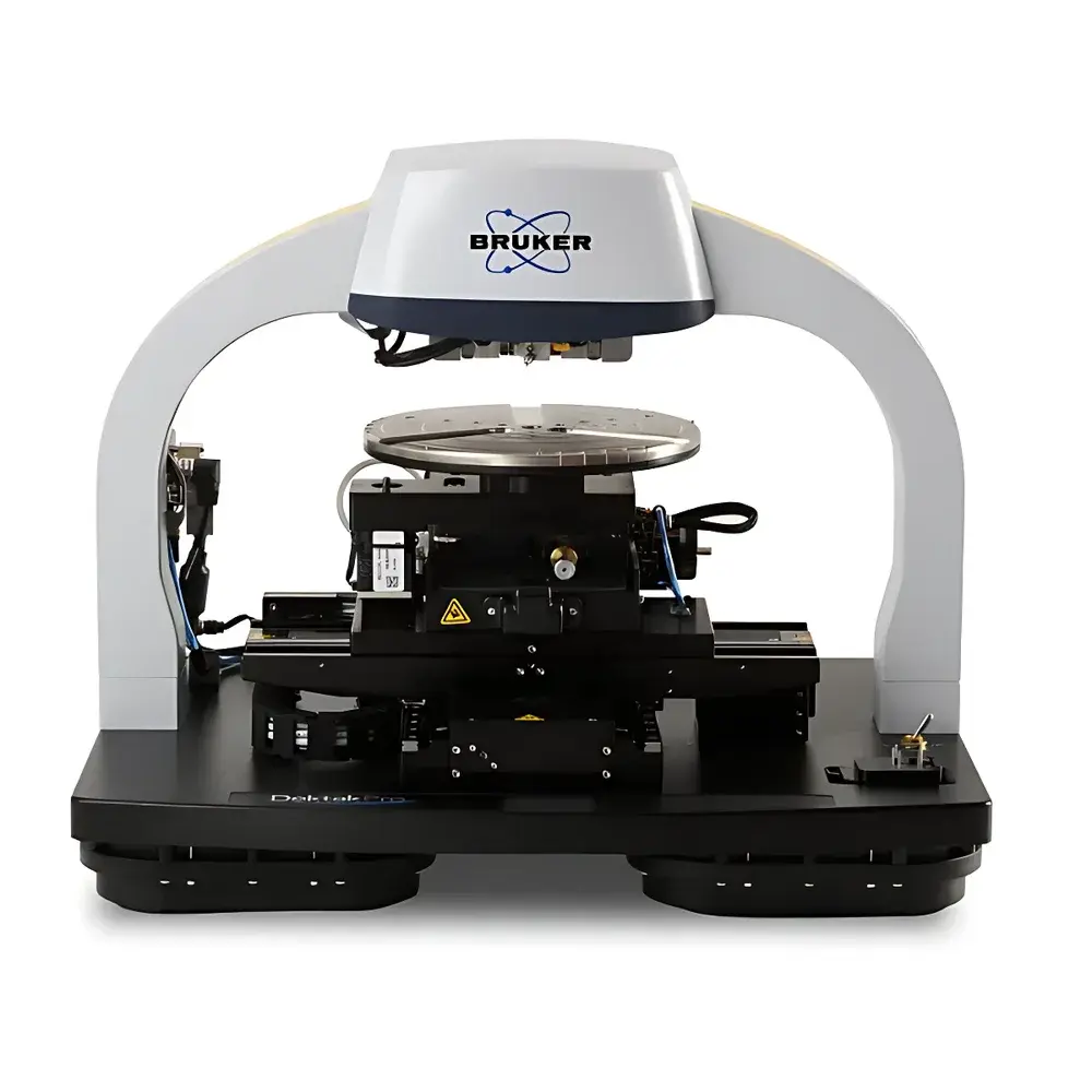
Bruker Dektak Pro Stylus Profilometer
| Brand | Bruker |
|---|---|
| Origin | Malaysia |
| Manufacturer Type | Authorized Distributor |
| Origin Category | Imported |
| Model | Dektak Pro |
| Measurement Principle | Contact Stylus Profilometry |
| Probe Normal Force | 0.03–15 mg (with N-Lite+ sensor) or 1–15 mg (standard LIS 3) |
| Scan Length | 55 mm (2") or 200 mm (8") with scan stitching capability |
| Step Height Repeatability | 4 Å, 1σ (on ≤1 μm certified step standard) |
| Vertical Resolution | 1 Å (at 6.55 μm vertical range) |
| Vertical Range | 1 mm |
| Maximum Data Points per Scan | 120,000 |
| Sample Thickness Capacity | up to 50 mm |
| Maximum Wafer Size | 200 mm (8") |
| XY Stage Options | Manual 100 mm (4"), Motorized 150 mm (6"), Encoder-equipped Motorized 200 mm (8") |
| Tip Radius Options | 50 nm – 25 μm |
| High-Aspect-Ratio (HAR) Tip | 200 μm × 20 μm |
| Field of View | 0.275–2.2 mm (via selectable optics) |
| Operating Temperature | 20–25°C |
| Relative Humidity | ≤80%, non-condensing |
| Input Voltage | 100–240 VAC, 50–60 Hz |
| Dimensions (Instrument) | 455 × 550 × 370 mm (W×D×H) |
| Weight | 34 kg |
Overview
The Bruker Dektak Pro is the eleventh-generation stylus profilometer engineered for high-precision, traceable surface topography characterization in research laboratories and advanced manufacturing environments. It operates on the principle of contact-based mechanical profiling: a diamond-tipped stylus traverses the sample surface under precisely controlled normal force, converting vertical displacement into high-fidelity analog voltage signals via a low-inertia sensor (LIS 3) or ultra-low-force N-Lite+ transducer. This analog signal is digitized at high sampling rates to reconstruct two-dimensional surface profiles with sub-angstrom vertical resolution—enabling quantitative analysis of step heights, film thickness, surface roughness (Ra, Rq, Rz), thin-film stress (via substrate curvature measurement), and wafer bow/warp. Designed for metrology-grade reproducibility, the Dektak Pro achieves 4 Å (0.4 nm) step height repeatability (1σ) on certified reference standards ≤1 μm in height—a performance benchmark validated under ISO 25178-601-compliant calibration protocols. Its modular architecture supports both R&D flexibility and production-floor robustness, making it suitable for applications governed by ASTM E1087, ISO 4287, ISO 25178-2, and SEMI MF1530 standards.
Key Features
- Ultra-low-force measurement capability: Selectable probe loading from 0.03 mg (N-Lite+) to 15 mg ensures compatibility with soft polymers, photoresists, biological films, and brittle semiconductor layers without plastic deformation or tip wear.
- Dual-scan-length platform: Standard 55 mm (2″) scanning range; optional 200 mm (8″) motorized stage with precision stitching algorithm enables seamless, calibrated profiling across full wafers or large-area substrates.
- High-density data acquisition: Up to 120,000 data points per single scan at user-defined lateral sampling intervals, preserving critical edge definition and nanoscale feature fidelity.
- Modular tip configuration: Interchangeable stylus options include radii from 50 nm to 25 μm and specialized high-aspect-ratio (HAR) tips (200 μm × 20 μm) for deep trench and sidewall characterization.
- Encoder-based motion control: Closed-loop, direct-drive scanning platform eliminates backlash and hysteresis, ensuring positional accuracy <±0.1 μm over full travel—critical for overlay-critical process development.
- Thermal and vibration stability: Optimized mechanical design, optional active vibration isolation, and strict environmental operating envelope (20–25°C, ≤80% RH) maintain metrological integrity during extended qualification runs.
Sample Compatibility & Compliance
The Dektak Pro accommodates substrates up to 200 mm in diameter and 50 mm in thickness, supporting silicon, sapphire, glass, metal foils, flexible electronics, and bio-substrates. Its manual or motorized 360° rotation stage enables azimuthal profiling and anisotropic stress mapping. All measurements adhere to Good Laboratory Practice (GLP) and Good Manufacturing Practice (GMP) requirements when configured with audit-trail-enabled software. System compliance includes alignment with ISO/IEC 17025 calibration traceability frameworks, ASTM F1530 for semiconductor wafer flatness, and USP for pharmaceutical coating uniformity assessment. Optional NIST-traceable step-height standards and factory-certified calibration reports are available for regulated industries requiring documented metrological assurance.
Software & Data Management
Bruker’s Vision64 software provides intuitive, workflow-driven operation—from automated multi-site measurement routines to advanced spectral analysis (PSD), curvature fitting, and stress calculation (Stoney equation). Data files conform to ASTM E1392-compliant ASCII formats and support direct export to MATLAB, Python (via HDF5), and statistical process control (SPC) platforms. Role-based user permissions, electronic signatures, and full 21 CFR Part 11-compliant audit trails—including operator ID, timestamp, parameter lock status, and raw waveform logging—are enabled by default in regulated deployment modes. Batch reporting templates comply with internal quality documentation systems and external customer deliverables (e.g., PPAP, FAI).
Applications
- Microelectronics: Critical dimension verification of etched trenches, CMP endpoint detection, interlayer dielectric thickness, and BEOL metal stack step coverage.
- Optical coatings: Quantification of layer uniformity, edge roll-off, and multilayer interference structure integrity on lenses and laser mirrors.
- MEMS/NEMS fabrication: Characterization of release etch depth, anchor geometry, and suspended beam deflection profiles.
- Advanced packaging: Underfill fillet height, solder bump coplanarity, and TSV (through-silicon via) recess measurement.
- Life sciences: Topographic mapping of cell-seeded scaffolds, hydrogel swelling kinetics, and drug-eluting stent coating thickness gradients.
- Materials science: Thin-film stress evolution during thermal cycling, oxidation layer growth kinetics, and atomic-layer-deposited (ALD) conformality assessment.
FAQ
What metrological standards does the Dektak Pro support for calibration and traceability?
The system supports ISO/IEC 17025 traceable calibration using NIST SRM 1970 and 1971 step-height standards. Factory certification includes uncertainty budgets per ISO/IEC Guide 98-3 (GUM).
Can the Dektak Pro perform automated multi-point measurements across a full 200 mm wafer?
Yes—when equipped with the encoder-motorized 200 mm stage and Vision64’s wafer mapping module, it executes programmable grid-based profiling with auto-focus, tip approach validation, and pass/fail thresholding per site.
Is third-party software integration supported for custom data analysis pipelines?
Yes—Vision64 provides COM API and Python SDK access to raw profile data, instrument state variables, and measurement metadata, enabling integration with LabVIEW, JMP, or enterprise MES/QMS platforms.
How is probe wear monitored and compensated during long-term operation?
The system logs cumulative scan distance and force history per tip. Vision64 includes tip wear diagnostic tools (edge sharpness degradation index) and automatic recalibration prompts based on drift thresholds defined in ASTM E1087 Annex A3.
Does the Dektak Pro meet requirements for ISO 13805:2021 (surface texture — areal methods)?
While primarily a 2D profilometer, optional 3D stitching mode combined with Vision64’s areal reconstruction algorithms satisfies ISO 13805 Annex B for quasi-areal evaluation of structured surfaces such as micro-lens arrays or textured solar cells.