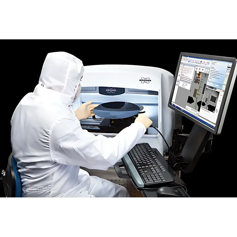
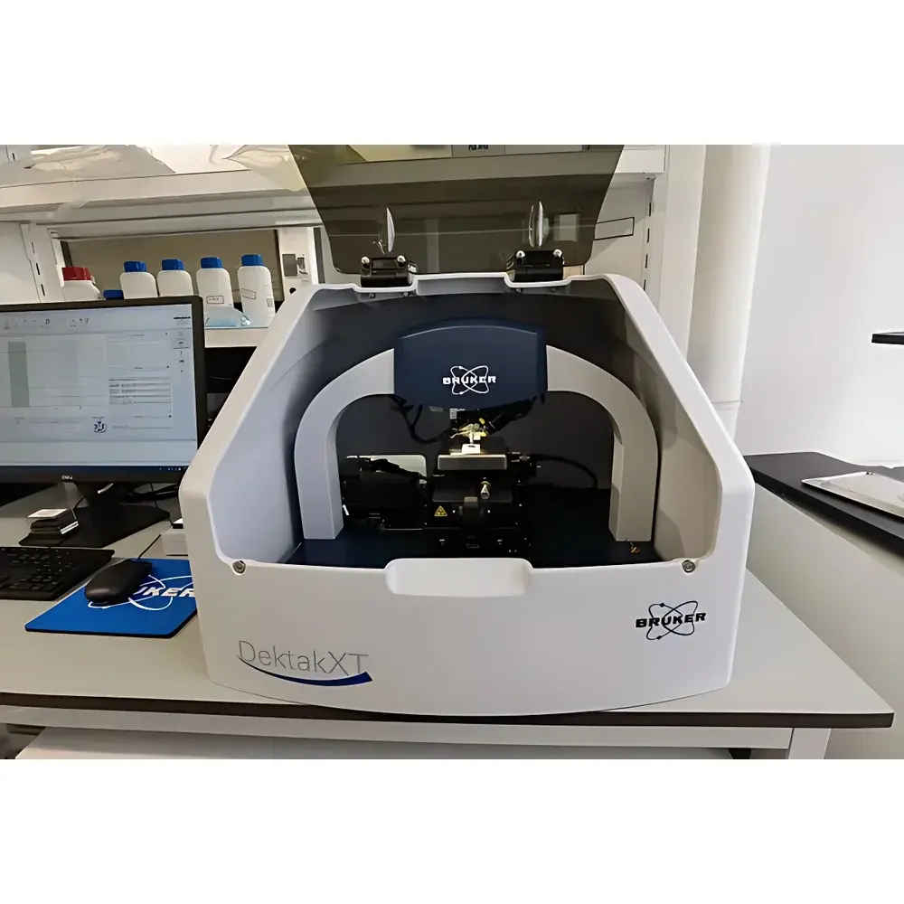
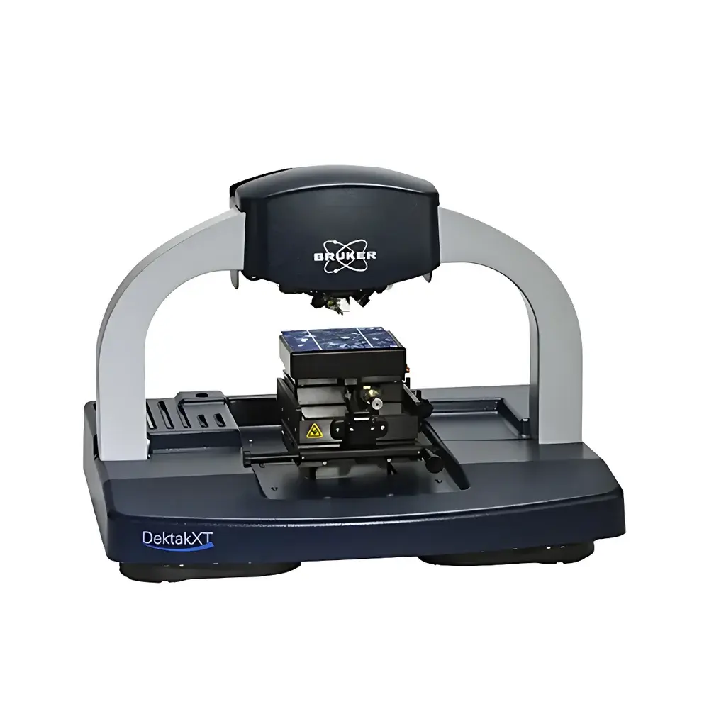
Bruker Dektak XT Stylus Profilometer
| Brand | Bruker |
|---|---|
| Origin | Germany |
| Manufacturer Type | Authorized Distributor |
| Origin Category | Imported |
| Model | Dektak XT |
| Measurement Principle | Capacitive Transduction |
| Vertical Repeatability | ≤ 5 Å |
| Vertical Resolution | 1 Å |
| Probe Tip Radius | 50 nm – 25 µm |
| Normal Force | 15 µN |
| Scan Length | 55 mm (2-inch) |
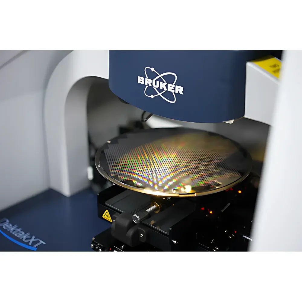
| Maximum Sample Size | 50 mm |
| Operating Temperature | 10–30 °C |
Overview
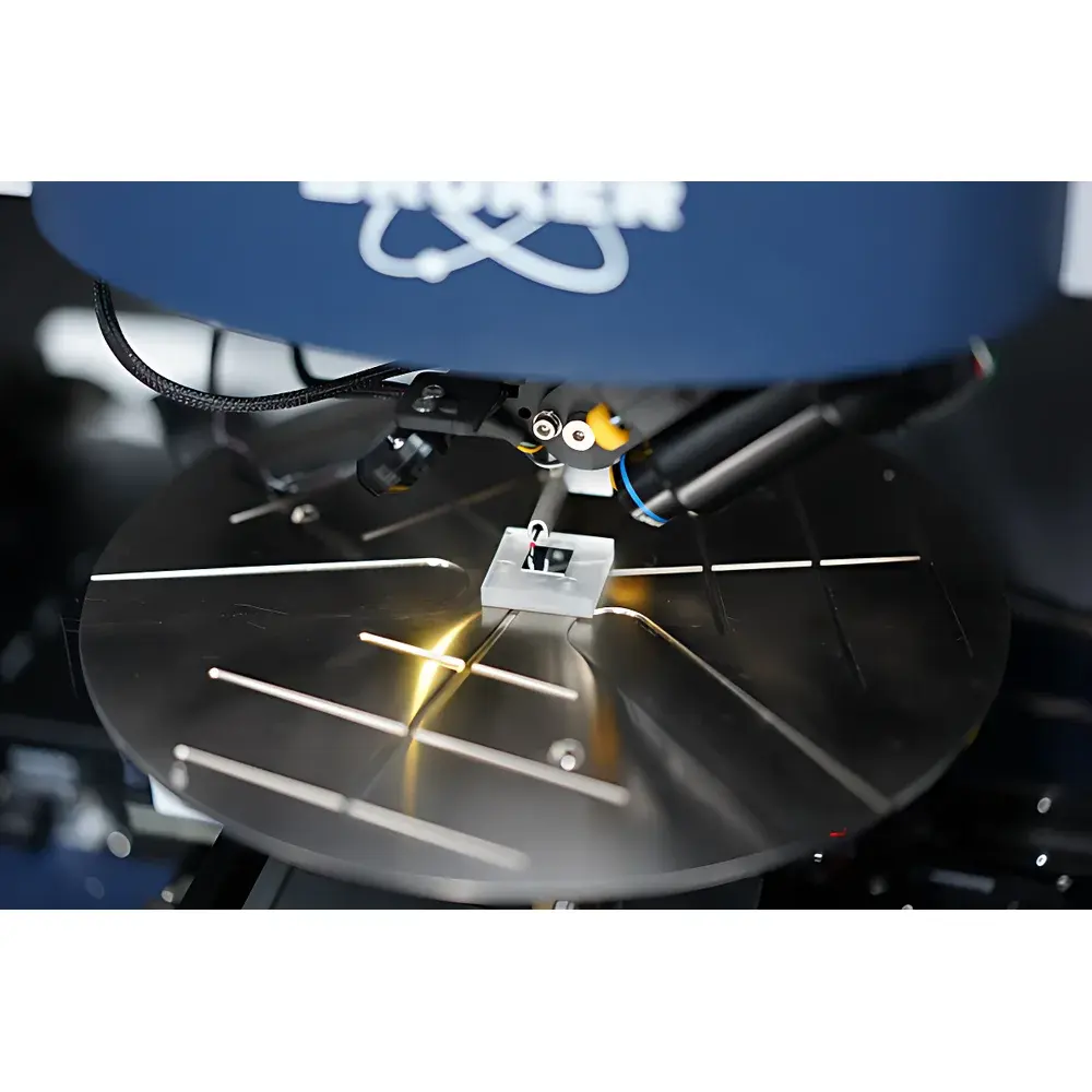
The Bruker Dektak XT is a high-precision, single-arch stylus profilometer engineered for nanoscale surface topography characterization. It operates on capacitive transduction principles—where vertical displacement of a diamond-tipped probe induces a measurable change in capacitance—enabling sub-angstrom vertical resolution and exceptional measurement stability. Designed as the tenth-generation evolution of Bruker’s Dektak platform, the Dektak XT integrates direct-drive scanning mechanics, integrated true-color HD optical imaging, and a proprietary 64-bit parallel processing architecture to deliver industry-leading repeatability (≤ 5 Å step height repeatability) and throughput. Its robust mechanical design minimizes thermal drift and vibration sensitivity, making it suitable for both R&D laboratories and production-integrated metrology environments where traceable, GLP-compliant surface quantification is required.
Key Features
- Single-arch mechanical architecture ensuring long-term scanning stability and minimal deflection across the full 55 mm scan range
- Capacitive transducer with 1 Å vertical resolution and ≤ 5 Å step height repeatability—validated per ISO 25178-6 and ASTM E1099 practices
- Automated tip calibration system with real-time force feedback, maintaining consistent 15 µN normal force across varying surface slopes and materials
- Integrated HD optical camera (1.3 MP, true-color) co-aligned with probe path for precise feature targeting and contextual overlay of topography data
- Direct-drive linear motor stage eliminating belt-driven hysteresis and enabling rapid, high-fidelity scans—even over extended 3D topographies or stress-induced curvature profiles
- Low-noise “Smart Electronics” architecture reducing electronic baseline drift and improving signal-to-noise ratio by >40% versus prior generations
- Probe tip radius configurable from 50 nm to 25 µm, supporting applications ranging from atomic-layer thin films to machined metallic surfaces
Sample Compatibility & Compliance
The Dektak XT accommodates wafers and substrates up to 50 mm in diameter, including silicon, sapphire, glass, polymer films, battery anodes/cathodes, and compound semiconductor heterostructures. Its non-destructive, low-force operation (15 µN nominal) ensures integrity of soft materials such as photoresists, organic LEDs, and thin-film solar absorbers. The system complies with ISO/IEC 17025 calibration traceability requirements when used with NIST-traceable step height standards. Data acquisition and reporting workflows support FDA 21 CFR Part 11 compliance via Vision64’s audit trail, electronic signatures, and secure user-role permissions—essential for regulated QC/QA environments in semiconductor manufacturing and medical device development.
Software & Data Management
Vision64 is Bruker’s native 64-bit, multi-threaded software platform optimized for real-time profilometry data acquisition, filtering, and analysis. It enables simultaneous acquisition and processing—accelerating 3D surface reconstruction by up to 10× compared to legacy 32-bit systems. Built-in filters include Gaussian, Spline, Robust, and ISO 16610 series operators; analysis modules cover step height, roughness (Sa, Sq, Sz), curvature, slope, bearing ratio (Abbott-Firestone), and film stress (Stoney equation integration). All reports are exportable in PDF, CSV, and Metrology Markup Language (MML) formats. Vision64 supports automated batch processing, script-driven multi-scan routines, and seamless integration with LIMS and MES platforms via OPC UA and RESTful API interfaces.
Applications
- Semiconductor process control: gate oxide thickness uniformity, CMP endpoint detection, lithographic resist profile metrology
- Microelectronics: MEMS structural deformation, TSV depth profiling, solder bump coplanarity assessment
- Battery R&D: cathode/anode coating thickness variation, calendering-induced surface texture, SEI layer growth kinetics
- Optoelectronics: GaN-based LED epitaxial layer step heights, AR/HR coating stack profiling
- Advanced materials: 2D material flake thickness mapping, graphene layer counting, polymer blend phase separation quantification
- Quality assurance: surface finish validation per ISO 4287/4288, wear track depth measurement, tribological interface characterization
FAQ
What is the minimum detectable step height on the Dektak XT?
The system achieves ≤ 5 Å repeatability for step height measurements under controlled environmental conditions (10–30 °C, <40% RH, vibration-isolated bench). Absolute minimum resolvable step depends on noise floor, tip geometry, and surface reflectivity—but routinely resolves features below 10 Å in optimized configurations.
Does the Dektak XT support automated multi-point mapping?
Yes—Vision64 includes grid-based auto-positioning routines compatible with motorized X-Y stages (optional). Users define coordinate arrays, dwell times, and analysis templates for unattended wafer-level or substrate-level mapping.
Is the system compliant with GMP/GLP documentation requirements?
When configured with Vision64’s Part 11 module, the system provides full audit trail logging, electronic signatures, and data integrity controls aligned with ICH-GCP, ISO 13485, and EU Annex 11 expectations.
Can the Dektak XT measure curved or non-planar substrates?
The single-arch design and dynamic tilt compensation algorithm enable accurate profiling on gently curved surfaces (radius ≥ 50 mm); for highly convex/concave geometries, optional curvature correction modules are available.
What calibration standards are recommended for routine verification?
Bruker recommends NIST-traceable step height standards (e.g., VLSI Standards SRM 2100 series) and certified roughness specimens (e.g., PTB BK-7 reference samples) for daily performance verification per ISO 21570.