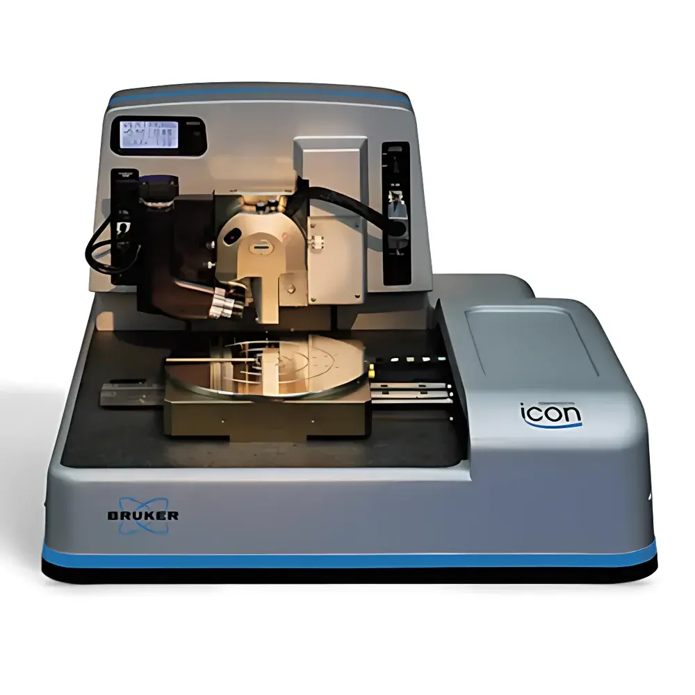
Bruker Dimension Icon Atomic Force Microscope
| Brand | Bruker |
|---|---|
| Origin | Germany |
| Manufacturer Type | Authorized Distributor |
| Origin Category | Imported |
| Model | Dimension Icon |
| Price Range | USD 135,000 – 205,000 (est.) |
| Instrument Type | Atomic Force Microscope |
| Application Class | Materials Science AFM |
| Position Detection Noise | <0.15 nm RMS (at typical imaging bandwidth up to 625 Hz) |
| Sample Diameter | Up to 210 mm |
| Sample Thickness Limit | ≤5 mm |
| XY Stage Travel Range | 180 mm × 150 mm |
| XY Repeatability | 2 µm (unidirectional), 3 µm (bidirectional) |
Overview
The Bruker Dimension Icon is a high-performance, open-architecture atomic force microscope engineered for quantitative nanoscale characterization of materials surfaces in academic, industrial, and governmental research laboratories. Operating on the principle of mechanical probe–surface interaction, the Dimension Icon employs a laser beam deflection detection system coupled with low-noise electronics to resolve topographic, mechanical, electrical, and magnetic properties at sub-nanometer resolution. Its design centers on robust scanning mechanics, minimized thermal drift, and optimized acoustic isolation—critical for long-duration, high-stability imaging and force spectroscopy experiments. As a materials-focused AFM platform, it supports both contact and dynamic modes (including tapping, peak-force tapping, and frequency modulation), enabling correlative analysis across diverse sample classes—from polymers and thin films to 2D materials and biological specimens under ambient or controlled environmental conditions.
Key Features
- Open-access probe–sample architecture facilitating rapid tip exchange, in situ optical access, and integration with external stimuli (e.g., temperature stages, electrochemical cells, or optical excitation sources)
- Low-position-detection-noise performance (<0.15 nm RMS at up to 625 Hz bandwidth), enabling high-fidelity imaging of soft and heterogeneous surfaces without excessive averaging
- Large-area XY stage (180 mm × 150 mm travel) accommodating wafers up to 210 mm in diameter and substrates up to 5 mm thick—ideal for semiconductor metrology, coating uniformity mapping, and cross-sectional device analysis
- Sub-micron stage repeatability (2 µm unidirectional, 3 µm bidirectional) supporting automated multi-site acquisition, stitching, and statistical surface metrology per ISO 25178 and ASTM E2947 standards
- Intuitive NanoScope software with pre-configured application workflows (e.g., “Polymer Phase Imaging”, “Nanomechanical Mapping”, “Conductive AFM”) reducing parameter optimization time from hours to seconds
- Modular hardware expansion support for advanced techniques including Kelvin probe force microscopy (KPFM), magnetic force microscopy (MFM), scanning capacitance microscopy (SCM), and nanolithography
Sample Compatibility & Compliance
The Dimension Icon accommodates rigid and compliant samples across a broad range of physical forms: polished wafers, cleaved crystals, spin-coated polymer films, freeze-dried biomaterials, and metallized MEMS devices. Its large sample stage and height-adjustable Z-sensor allow direct mounting of standard SEM stubs, custom holders, or environmental chambers. The system complies with CE marking requirements and meets electromagnetic compatibility (EMC) standards per EN 61326-1. For regulated environments—including GLP-compliant materials testing labs and GMP-aligned R&D facilities—the NanoScope software optionally supports 21 CFR Part 11–compliant audit trails, electronic signatures, and user-role-based access control when deployed with Bruker’s NanoScope Analysis Suite.
Software & Data Management
NanoScope software provides a unified interface for instrument control, real-time data visualization, and post-acquisition quantification. It features embedded scripting (via Python API), batch processing pipelines, and native support for industry-standard file formats (e.g., Gwyddion-compatible .gws, SPIP-readable .spm, and HDF5 export). All raw sensor signals—including photodiode quadrants, Z-piezo voltage, and drive amplitude/phase—are recorded with timestamped metadata. Data integrity is preserved through automatic checksum validation, versioned project archives, and optional network-attached storage (NAS) synchronization. For collaborative analysis, Bruker offers cloud-enabled data sharing via NanoScope Cloud Connect—a secure, encrypted portal supporting role-based viewing, annotation, and comparative overlay of multi-modal datasets.
Applications
- Surface roughness and waviness quantification of optical coatings and precision optics per ISO 10110-8
- Nanoscale phase separation analysis in block copolymers and polymer blends
- Mechanical property mapping (modulus, adhesion, deformation) of battery electrode composites and solid electrolytes
- Defect identification and critical dimension metrology on EUV lithography masks and FinFET structures
- In situ electrochemical AFM of SEI layer evolution during Li-ion cell cycling
- Topographic and potential mapping of graphene domains and transition metal dichalcogenide monolayers
FAQ
What environmental conditions are recommended for optimal Dimension Icon performance?
A vibration-isolated optical table, temperature stability ±0.5°C/hour, and relative humidity between 30–60% (non-condensing) are advised. Acoustic noise below 45 dB(A) and absence of strong magnetic fields (>1 mT) are required for low-drift operation.
Is the Dimension Icon compatible with non-Bruker probes?
Yes—it accepts standard 125 µm–wide cantilevers with reflective backside coating (e.g., BudgetSensors, Nanoworld, Olympus-type), provided they meet the specified resonance frequency range (15–300 kHz) and optical alignment tolerances.
Can the system be upgraded for vacuum or liquid imaging?
Vacuum-compatible versions (Dimension Icon UHV) and fluid cell modules (Dimension Icon Fluid Cell Kit) are available as factory-installed options, each requiring dedicated calibration and safety interlocks.
Does Bruker provide application-specific training and method development support?
Yes—Bruker’s Applications Scientists offer on-site and remote workshops covering technique selection, parameter optimization, artifact diagnosis, and ISO/ASTM-compliant reporting templates.


