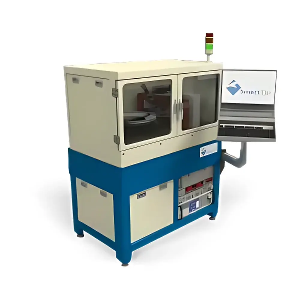
Bruker SmartProber-P1 Tunneling Magnetoresistance (TMR) Measurement System
| Brand | Bruker |
|---|---|
| Origin | USA |
| Manufacturer Type | Authorized Distributor |
| Product Origin | Imported |
| Model | SmartProber-P1 |
| Magnetic Field Configuration | 6 kOe vertical-field permanent magnet |
| Wafer Handling | Motorized 300 mm rotating wafer stage |
| TMR Resistance-Area Product Range | 0.1–100 kΩ·µm² |
| Optional Modules | In-plane 2 kOe magnet (C), 200 mm XY stage (Y), Manual sample stage (M), 10 kOe vertical magnet (L) |
Overview
The Bruker SmartProber-P1 is a precision-engineered tunneling magnetoresistance (TMR) measurement system designed for semiconductor R&D, process development, and failure analysis laboratories requiring quantitative characterization of magnetic tunnel junctions (MTJs) on full 300 mm wafers. Operating on the principle of current-in-plane tunneling (CIPT) and current-perpendicular-to-plane (CPP) resistivity extraction, the SmartProber-P1 integrates a high-stability 6 kOe vertical-field permanent magnet with a motorized, vacuum-compatible 300 mm rotating wafer stage to enable spatially resolved, non-destructive TMR and RA (Resistance × Area) mapping across entire wafers. Its modular architecture supports both production-integrated metrology workflows and exploratory research on emerging spintronic materials—including CoFeB/MgO-based MTJs, synthetic antiferromagnetic (SAF) pinned layers, and voltage-controlled magnetic anisotropy (VCMA) structures. The system complies with industry-standard wafer handling protocols (SEMI E10, E142) and is engineered for long-term stability under cleanroom Class 100 conditions.
Key Features
- High-field vertical magnet (6 kOe standard; optional 10 kOe upgrade) delivering uniform field distribution over ≥95% of 300 mm wafer diameter
- Motorized rotating wafer stage with ±0.005° angular repeatability and integrated edge-detection alignment for automated die-level positioning
- RA measurement range spanning 0.1–100 kΩ·µm², optimized for sub-20 nm node MTJ stacks with sub-1 nm MgO barrier thickness control
- Modular configuration options: in-plane 2 kOe magnet module (C) for exchange-bias or anisotropic magnetoresistance (AMR) studies; 200 mm XY translation stage (Y) for small-format substrates; manual sample holder (M) for rapid prototyping of discrete devices
- Low-noise, guarded four-point probe head with active thermal drift compensation and <10 fA base current resolution
- Integrated vibration-isolated granite base and electromagnetic shielding enclosure compliant with IEEE Std 291–2020 for low-signal integrity environments
Sample Compatibility & Compliance
The SmartProber-P1 accommodates standard 300 mm silicon wafers with front-side flat or notch orientation, as well as 200 mm wafers and diced dies mounted on carrier frames. It supports blanket films, patterned arrays, and test structures conforming to JEDEC JESD22-A108 (temperature cycling) and JESD22-A110 (high-temperature storage) preconditioning requirements. All electrical measurements adhere to ASTM F2718–22 (Standard Test Method for Electrical Characterization of Magnetic Tunnel Junctions) and are traceable to NIST SRM 1265a (low-resistance standard). System firmware and data acquisition logs support audit-ready GLP/GMP documentation, including electronic signatures and 21 CFR Part 11–compliant audit trails when paired with Bruker’s certified LabScape™ software suite.
Software & Data Management
Control and analysis are performed via Bruker’s proprietary ProberControl™ v4.2 software, a Windows-based platform featuring real-time RA mapping visualization, automated field-sweep sequencing (0–±6 kOe in 1 Oe steps), and multi-parameter curve fitting (e.g., Slonczewski–Berger switching models, Julliere TMR ratio extraction). Raw data are stored in HDF5 format with embedded metadata (wafer ID, timestamp, environmental sensor readings, calibration coefficients). Export modules support CSV, MATLAB .mat, and ICV-compatible formats for integration into factory MES systems. Remote monitoring and script-driven batch processing are enabled through Python 3.9 API bindings compliant with PEP 561 type hints.
Applications
- RA and TMR uniformity mapping across 300 mm wafers for MRAM process qualification
- Barrier quality assessment via RA vs. thickness correlation on MgO/CoFeB stacks
- Exchange bias field quantification in SAF-based reference layers using in-plane + perpendicular field vector combinations
- Thermal stability (ΔE/kBT) evaluation via temperature-dependent RA sweeps from 10 K to 400 K (with optional cryo-chuck)
- Fault isolation of localized pinholes or interfacial oxidation in tunnel barriers using spatially resolved I–V hysteresis imaging
- Qualification of VCMA coefficients (dP/dV) in gate-tunable MTJs under combined electric and magnetic fields
FAQ
What is the minimum measurable RA value with the SmartProber-P1?
The system achieves reliable RA detection down to 0.1 kΩ·µm² under optimized probe contact conditions and low-noise grounding configurations.
Can the SmartProber-P1 measure both parallel and anti-parallel resistance states simultaneously?
Yes—field-sweep mode captures full R(H) loops with programmable sweep direction, rate, and dwell time, enabling direct extraction of RP, RAP, and TMR = (RAP−RP)/RP.
Is the 300 mm stage compatible with SMIF pods or FOUPs?
The system interfaces with standard 300 mm load ports per SEMI E47.1 and supports automated transfer via third-party robotic handlers equipped with SECS/GEM communication.
Does Bruker provide calibration services traceable to national standards?
Yes—annual calibration packages include NIST-traceable resistance and field strength verification, documented per ISO/IEC 17025:2017 by Bruker’s A2LA-accredited metrology lab.
How is data integrity maintained during extended overnight measurements?
ProberControl™ implements checksummed data streaming, automatic resume-on-interrupt, and dual-redundant SSD logging to prevent corruption during multi-hour RA mapping sequences.


