
Cascade Microtech EPS Series Manual Probe Station
| Origin | USA |
|---|---|
| Manufacturer Type | Authorized Distributor |
| Origin Category | Imported |
| Model | EPS Series |
| Price Range | USD $65,000 – $130,000 (FOB USA) |
| Product Category | RF-Compatible Manual Probe Station |
| Operation Mode | Manual |
| Base Platform | 150 mm Wafer-Capable |
| Max XY Travel | 155 mm × 155 mm |
| Minimum Positioning Resolution | 5 µm |
| Theta Rotation | 360° Continuous |
| Z-Axis Vertical Travel | 10 mm |
| Standard Base Dimensions | 490 mm × 490 mm × 480 mm (W × D × H) |
Overview
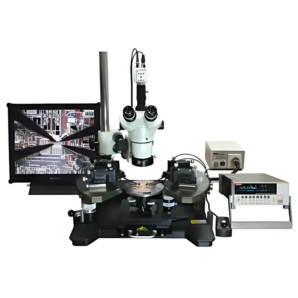
The Cascade Microtech EPS Series Manual Probe Station is an engineered precision measurement platform designed for semiconductor device characterization, failure analysis (FA), and wafer-level reliability (WLR) testing. Built upon a robust mechanical architecture and grounded in proven micro-positioning principles, the EPS employs a high-stiffness, low-drift X-Y-θ stage system with sub-5 µm repeatability—enabling stable, repeatable contact alignment for DC, low-frequency AC, and RF probing applications up to 67 GHz (when equipped with compatible RF probes and shielding). Its 150 mm (6-inch) wafer-compatible base platform supports full-die probing across silicon, compound semiconductors (e.g., GaAs, SiC), MEMS, photonic integrated circuits (PICs), and microfluidic substrates. Unlike monolithic probe stations, the EPS utilizes a modular mechanical and electrical interface framework—allowing users to configure only the subsystems required for current test needs while preserving upgrade paths for future requirements including thermal, optical, or high-frequency extensions.
Key Features
- Modular mechanical architecture: Interchangeable stages, chuck types (flat, vacuum, heated), and probe arm mounts enable application-specific configuration without system replacement.
- High-precision X-Y-θ motion: 155 mm × 155 mm travel range with 5 µm minimum step resolution and continuous 360° rotational capability for angular alignment of RF probes or asymmetric devices.
- RF-optimized structural design: Integrated grounding planes, low-inductance base construction, and optional RF head modules support impedance-controlled probing environments compliant with IEEE 169 and IPC-9701 guidelines.
- Expandable environmental integration: Native mounting interfaces for thermal chucks (ambient to +300°C), EMI/RFI-shielded enclosures, coaxial RF feedthroughs, and high-magnification CCD-based video microscopy systems (up to 1000× digital zoom).
- Probe card compatibility: Dedicated probe card port (PCP) interface enables direct integration with industry-standard probe cards for wafer-level burn-in and reliability stress testing under JEDEC JESD22-A108 conditions.
- Failure analysis readiness: Optional laser voltage probing (LVP) and electro-optical emission (EOE) ports support time-resolved fault isolation per SEMI F20 and JEDEC JESD22-A115 standards.
Sample Compatibility & Compliance
The EPS platform accommodates a broad spectrum of sample formats: bare die (single-chip), 150 mm wafers (standard), PCB assemblies, ceramic packages, MEMS sensors, and glass/microfluidic substrates up to 20 mm thickness. Vacuum chucks provide uniform clamping for thin or warped wafers; optional edge-clamp solutions are available for non-vacuum-compatible materials. All mechanical and electrical configurations adhere to ISO 9001-certified manufacturing practices. When configured with RF modules and shielded enclosures, the system meets FCC Part 15 Class B emissions limits and supports GLP-compliant test documentation workflows. Full traceability of stage position logs, temperature setpoints, and probe contact events is maintained via optional audit-trail-enabled software (compliant with FDA 21 CFR Part 11 Annex 11 requirements).
Software & Data Management
While the EPS operates manually at the hardware level, it integrates seamlessly with third-party automation and data acquisition platforms—including Cascade’s WinCal™ calibration suite, Keysight PathWave ADS, and Python-based PyVISA instrument control frameworks. Position coordinates (X, Y, θ, Z) are accessible via RS-232 or USB-to-serial interfaces for synchronization with oscilloscopes, SMUs, VNAs, and parameter analyzers. Optional EPS-FA software add-ons provide structured FA workflow templates, annotated image capture (with timestamped metadata), and CSV/Excel-exportable contact log files—including probe force estimation, touchdown detection timestamps, and thermal drift compensation records. All exported datasets conform to ASTM E2917-21 data formatting conventions for semiconductor parametric testing.
Applications
- DC parametric characterization of transistors, diodes, and passive structures on 150 mm wafers or diced die.
- RF S-parameter extraction using calibrated ground-signal-ground (GSG) probes, supporting de-embedding per IEEE P370.
- Wafer-level reliability (WLR) stress testing—including HTGB, TDDB, and HCI—using probe-card-mounted test structures.
- MEMS actuator characterization requiring synchronized optical observation and electrical stimulus.
- Photonic device testing (e.g., grating couplers, modulators) with integrated near-field optical access ports.
- Failure analysis root-cause localization via emission microscopy (EMMI), OBIRCH, or laser-assisted device alteration (LADA).
FAQ
Is the EPS Series compatible with automated wafer handling?
No—the EPS is a manual probe station by design. For semi-automated or fully automated operation, consider Cascade’s Summit series or FormFactor’s Cascade Microtech AutoProber platform.
What RF frequency range is supported out-of-the-box?
The base EPS platform supports DC–1 GHz measurements. With optional RF head modules, SMA/K-type connectors, and shielded enclosure integration, performance extends to 67 GHz (dependent on probe selection and calibration method).
Can I retrofit my existing EPS with a thermal chuck?
Yes—thermal chucks (ambient to +300°C) are field-installable using standard M4 mounting threads and compatible with all EPS generations post-2015.
Does the EPS meet cleanroom compatibility requirements?
Standard EPS frames are constructed from anodized aluminum and stainless steel with non-outgassing elastomers. Optional cleanroom-grade versions (ISO Class 5 compliant) feature electropolished surfaces and particle-trapped cable management.
Is technical support and calibration documentation provided internationally?
Yes—authorized distributors supply NIST-traceable stage calibration certificates, ISO/IEC 17025-compliant service reports, and remote application engineering support in English, German, Japanese, and Mandarin.


