Filmetrics F20 Desktop Thin-Film Thickness Metrology System
| Brand | KLA-Filmetrics |
|---|---|
| Origin | USA |
| Manufacturer Type | Authorized Distributor |
| Import Status | Imported |
| Model | F20 |
| Price Range | USD $28,000–$50,000 |
| Measurement Principle | Spectral Reflectance Interferometry |
| Thickness Range | 15 nm – 450 µm |
| Thickness Resolution | ≤0.1 nm (1 Å) |
| Thickness Repeatability | ±0.7 Å |
| Measurement Time | 1–2 s per spot |
| Spectral Range Options | 200–1700 nm (configurable by model variant: UV, VIS-NIR, EXR, NIR) |
| Sample Compatibility | Smooth, transparent or semi-transparent films on reflective or transmissive substrates |
| Optical Constants Measured | n (refractive index), k (extinction coefficient), surface roughness (via effective medium approximation) |
| Software Platform | Filmetrics F20™ Suite (Windows-based, USB-connected) |
| Compliance | Supports GLP/GMP audit trails, ASTM E2386-22 (Standard Practice for Spectral Reflectance-Based Film Thickness Measurement), ISO/IEC 17025 traceable calibration protocols |
Overview
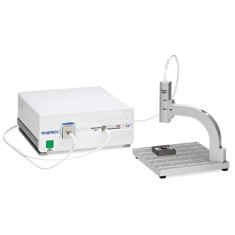
The Filmetrics F20 is a benchtop spectral reflectance metrology system engineered for rapid, non-contact, and high-reproducibility measurement of thin-film thickness and optical constants (n and k) across semiconductor, display, photovoltaic, optics, and advanced materials R&D and manufacturing environments. Operating on the physical principle of white-light interferometric reflectance, the F20 directs broadband light onto a sample surface; interference between reflections from the film’s top and substrate interfaces generates a wavelength-dependent reflectance spectrum. By fitting this measured spectrum to a physically accurate optical model—accounting for layer structure, dispersion, substrate properties, and surface roughness—the system solves for thickness, refractive index, extinction coefficient, and effective porosity in a single acquisition. Designed for integration into cleanroom labs and university teaching facilities alike, the F20 delivers sub-angstrom resolution (≤0.1 nm), repeatability better than ±0.7 Å, and full quantitative analysis in under two seconds per measurement point—without requiring vacuum, cryogenics, or complex alignment.
Key Features
- Single-button operation with real-time spectral acquisition and automated model fitting—no user-defined optical modeling expertise required.
- Modular spectral configurations: F20-UV (200–900 nm), F20-VIS (400–1000 nm), F20-EXR (400–1700 nm), and F20-NIR (900–1700 nm)—selected based on material absorption edges and target thickness range.
- USB-powered, portable design compatible with standard Windows™ PCs; no external power supplies or cooling units needed.
- Integrated sample stage with manual XYZ adjustment; optional motorized stages and auto-focus modules available for multi-point mapping.
- Proprietary algorithms for ITO, SiNx, porous Si, SU-8, and multilayer stacks—including Bruggeman effective medium modeling for nanocomposites and graded interfaces.
- Factory-calibrated using NIST-traceable standards; supports user-initiated recalibration with certified reference wafers.
Sample Compatibility & Compliance
The F20 measures smooth, continuous films ≥15 nm thick on rigid substrates including silicon, glass (borosilicate, fused silica), sapphire, quartz, and metal-coated wafers. It supports single-layer, bilayer, and up to four-layer transparent or semi-transparent stacks—provided sufficient optical contrast exists between layers. Common measurable materials include SiO2, SiNx, ITO, TiO2, Al2O3, Parylene-C, photoresists (SU-8, AZ series), liquid crystal layers, hard coatings (e.g., DLC, SiC), and porous silicon. The system complies with ASTM E2386-22 for spectral reflectance-based thickness measurement and supports instrument qualification documentation aligned with ISO/IEC 17025 requirements. Audit trail functionality—including operator ID, timestamp, parameter history, and raw spectrum export—is enabled within the F20 software suite to meet GLP and GMP data integrity expectations (aligned with FDA 21 CFR Part 11 principles for electronic records).
Software & Data Management
The Filmetrics F20™ software suite provides a deterministic, scriptable, and version-controlled environment for measurement setup, analysis, and reporting. All models are stored as editable XML files; spectral fits are saved with full metadata (wavelength range, detector gain, integration time, ambient temperature). Batch processing enables sequential measurements across wafer maps or production lots, with CSV and HDF5 export options for integration into MES or SPC platforms. The software includes built-in libraries for >200 materials—including dispersion models for crystalline and amorphous Si, ITO, SiNx (Si-rich to stoichiometric), and polymer substrates (PET, PC, PI). Custom material definitions can be added via Sellmeier or Cauchy parameter entry. Raw spectra and fit residuals are retained for root-cause analysis; uncertainty estimates (based on spectral noise floor and model sensitivity) are reported alongside each thickness value.
Applications
The F20 serves as a primary metrology tool across multiple high-precision industries. In semiconductor fabrication, it quantifies gate oxides (1–10 nm), anti-reflective coatings, and hard masks during process development and inline QC. In flat-panel display manufacturing, it measures ITO electrode thickness (30–200 nm), polyimide alignment layers, and cell gap uniformity in LCDs and OLEDs. Photovoltaic R&D labs use it to characterize CdTe/CdS absorber stacks on TEC glass and monitor TCO layer homogeneity. MEMS developers rely on its speed and accuracy for SU-8 structural layers (1–500 µm) and release etch monitoring. Academic institutions deploy F20 systems in undergraduate semiconductor processing labs—leveraging their intuitive interface and pedagogical clarity to demonstrate optical interference, dispersion modeling, and thin-film characterization fundamentals. Additional validated applications include ophthalmic lens coatings, web-coated polymer films (PET, PVC), and porous silicon biosensor development.
FAQ
What substrates are compatible with the F20?
The F20 requires optically flat, rigid substrates with minimal scattering—such as polished silicon wafers, fused silica, borosilicate glass, sapphire, and metal-coated mirrors. Flexible or highly diffusive substrates (e.g., paper, textured polymers) are not supported.
Can the F20 measure opaque or absorbing films?
Yes—within limits. Films with moderate absorption (e.g., metals <50 nm thick, doped oxides, organic semiconductors) can be modeled if their k-values are known or constrained. Highly absorbing films (e.g., bulk Cu, Al) require ellipsometry or XRF for reliable thickness determination.
Is calibration required before each use?
No. Factory calibration remains stable for ≥12 months under normal lab conditions. Users may perform verification checks using certified reference wafers (e.g., thermal SiO2/Si); full recalibration is recommended annually or after hardware service.
Does the F20 support automated wafer mapping?
The base F20 is a single-spot system. For mapping, users integrate it with third-party XY stages or upgrade to the F50 (blank wafer mapping) or F80 (product wafer mapping) platforms—both sharing identical optical engines and software architecture.
How does the F20 handle rough or patterned surfaces?
Surface roughness is modeled via effective medium approximation (EMA) in multilayer fits. For patterned samples (e.g., lithographically defined features), lateral resolution is limited by spot size (standard: ~30 µm; optional fiber-coupled probes down to 20 µm). Sub-micron features require the F40 configured with microscope coupling.


