GETec AFSEM™ In-Situ Atomic Force Microscopy System for Scanning Electron Microscopes
| Brand | GETec Microscopy |
|---|---|
| Origin | Austria |
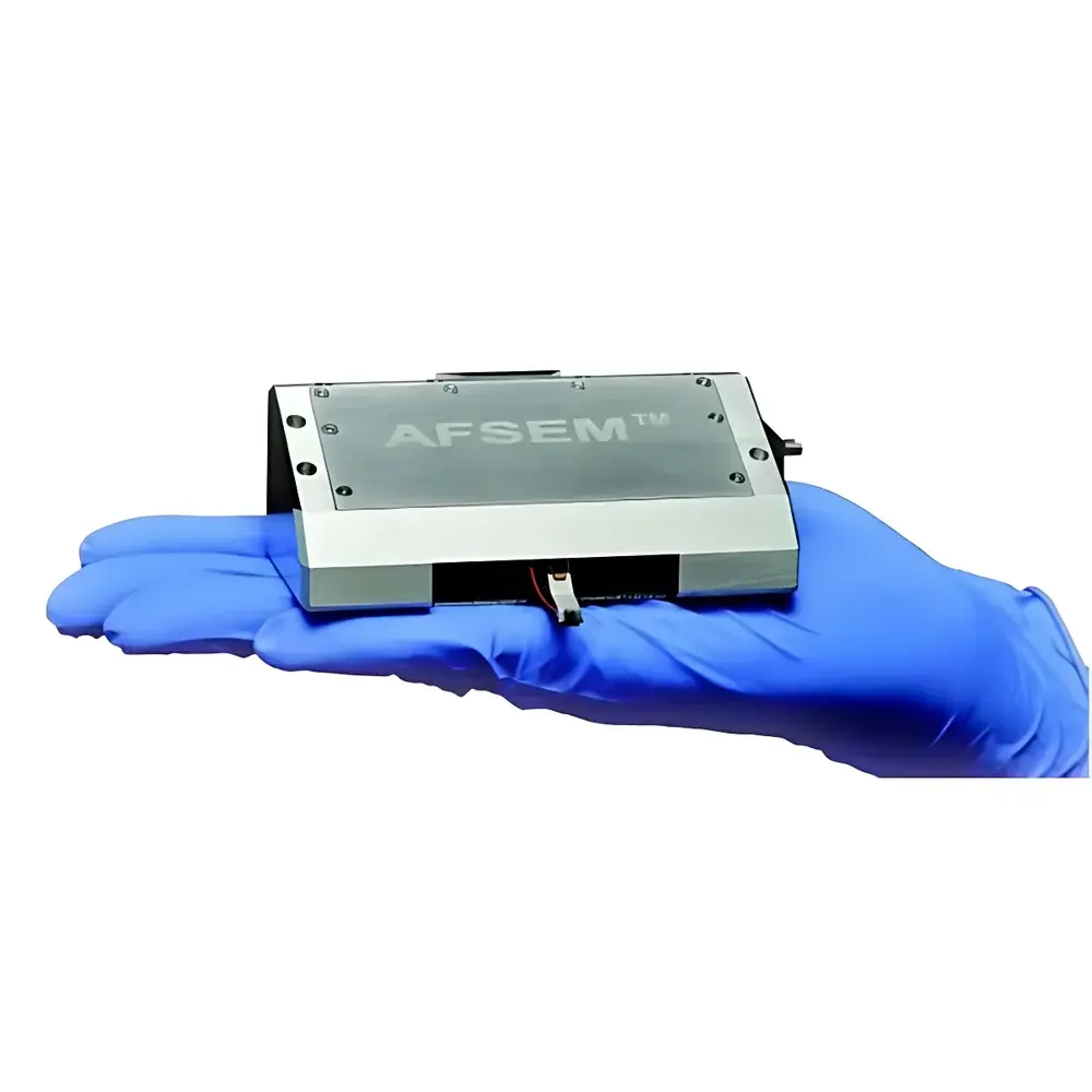
| Model | AFSEM |
| Instrument Type | In-Situ AFM Integration System for SEM |
| Sample Dimensions | H = 41 mm, L = 110 mm, W = 77 mm |
| Stage Travel Range | X = ±4 mm (±7.5 mm optional), Y = ±4 mm, Z = 25 mm |
Overview
The GETec AFSEM™ is an engineered in-situ atomic force microscopy (AFM) integration system designed specifically for vacuum-compatible scanning electron microscopes (SEMs). Unlike conventional standalone AFMs, the AFSEM operates *inside* the SEM chamber without compromising vacuum integrity, enabling true concurrent multimodal imaging and nanoscale characterization. It leverages piezoresistive self-sensing cantilever technology—eliminating the need for optical beam deflection—and thus avoids laser alignment constraints, optical path obstructions, and spatial limitations common in traditional AFM-SEM hybrids. The system implements a robust, compact mechanical architecture that mounts directly to the SEM chamber door or side port, preserving full access to standard SEM functionality—including EDS, EBSD, FIB, FEBID, and in-situ mechanical stages—while adding quantitative topographic, mechanical, and electrical surface metrology at sub-nanometer resolution. Its operational principle relies on direct piezoresistive transduction of cantilever bending, enabling high-bandwidth force feedback, stable tip–sample interaction control, and compatibility with both conductive and insulating samples under high-vacuum or low-vacuum (ESEM) conditions.
Key Features
- True in-situ, real-time co-imaging: Simultaneous SEM secondary/electron backscatter imaging and AFM topography, phase, force spectroscopy, and conductivity mapping—no sample transfer or vacuum break required.
- Self-sensing silicon cantilevers: Integrated piezoresistive full Wheatstone bridge eliminates optical detection; enables operation in confined SEM geometries (minimum tip–sample clearance: 4.5 mm).
- Modular stage integration: Compatible with standard SEM sample holders; retains full XYZ stage mobility (X/Y: ±4 mm, Z: 25 mm) and supports extended travel (±7.5 mm X/Y upon request).
- Vacuum-rated design: Fully bakeable to ≤10⁻⁶ mbar; compatible with high-resolution field-emission SEMs (e.g., Zeiss Leo 982, FEI Quanta 600 FEG ESEM, Philips XL40) and dual-beam FIB-SEM platforms.
- Multimodal AFM modes: Supports contact, tapping, force-volume, force modulation, current-sensing (CS-AFM), and lateral force microscopy—all operable within the SEM environment.
- Interchangeable probe library: Offers SCL-Sensor.Tech cantilevers with silicon tips (<15 nm radius), SCD tips (<10 nm radius), or tipless variants—each calibrated for stiffness (0.5–400 N/m), resonance frequency (14–1300 kHz), and application-specific performance.
Sample Compatibility & Compliance
The AFSEM accommodates standard SEM stub-mounted specimens up to 110 mm × 77 mm × 41 mm in volume, including fragile 2D materials (e.g., suspended graphene), MEMS devices, battery electrodes, catalysts, and metallurgical cross-sections. Its non-optical detection scheme ensures reliable operation on highly reflective, transparent, or topographically complex surfaces where laser-based AFMs suffer signal dropout or thermal drift. From a regulatory standpoint, AFSEM-acquired data supports GLP-compliant workflows when paired with audit-trail-enabled acquisition software (e.g., GETec’s AFSEM Control Suite v4.x). While the hardware itself does not carry CE/UKCA marking as a standalone medical or industrial device, its integration into ISO/IEC 17025-accredited SEM laboratories conforms to traceability requirements for nanoscale dimensional metrology per ISO/IEC 17025:2017 Annex A (Measurement Uncertainty) and ASTM E2527–21 (Standard Guide for AFM Calibration).
Software & Data Management
The AFSEM Control Suite provides synchronized, time-stamped acquisition of SEM image streams, AFM topography matrices, force curves, and spectroscopic datasets. All raw signals—including piezoresistive bridge output, Z-piezo displacement, and stage coordinates—are logged in HDF5 format with embedded metadata (timestamp, vacuum pressure, HV setting, detector gain). Software features include real-time overlay of AFM height maps onto SEM frames, region-of-interest (ROI) correlation tools, batch processing for force-volume arrays, and export to industry-standard formats (TIFF, Gwyddion, SPIP, MATLAB .mat). For regulated environments, optional 21 CFR Part 11 compliance packages are available—featuring electronic signatures, user role management, and immutable audit trails for all measurement parameters and post-processing steps.
Applications
- In-situ mechanical testing: Coupled with Deben 200N tensile stages in Philips XL40 SEM to quantify surface roughness evolution, grain boundary sliding, and necking dynamics during uniaxial loading.
- Nanoscale indentation & plasticity: Integrated with Hysitron PI85 nanoindenter in Zeiss Leo 982 SEM to correlate load-displacement curves with real-time AFM-measured pile-up, sink-in, and dislocation-mediated deformation.
- 2D material characterization: Layer-counting of freestanding graphene via low-kV SEM contrast, followed immediately by AFM height profiling and adhesion mapping—without breaking vacuum or relocating the region of interest.
- Electrochemical interface analysis: In-situ observation of SEI growth on Li-ion battery cathodes under controlled gas environments (ESEM mode), combined with conductive-AFM to map local ionic/electronic transport heterogeneity.
- Failure analysis of semiconductor interconnects: Correlating EDS elemental maps with AFM-derived line profiles of Cu diffusion barriers, void nucleation sites, and electromigration-induced surface undulations.
FAQ
Does AFSEM require modification to the SEM column or electron optics?
No. AFSEM mounts externally via the chamber door or side port and occupies no space within the electron optical path.
Can AFSEM operate in variable-pressure or ESEM mode?
Yes—its piezoresistive sensing is insensitive to water vapor or low-pressure gas environments, enabling stable operation down to 100 Pa in ESEM configurations.
Is calibration traceable to national standards?
Z-piezo calibration is performed using NIST-traceable interferometric stage references; cantilever spring constants are determined via Sader method with thermal noise analysis.
What is the minimum working distance required between tip and sample?
4.5 mm—enabling use with standard SEM objective lenses and long-working-distance detectors.
Are custom cantilevers supported?
Yes. GETec provides OEM integration support for application-specific cantilevers, including high-stiffness probes for nanoindentation or ultra-low-noise variants for sub-piconewton force spectroscopy.


