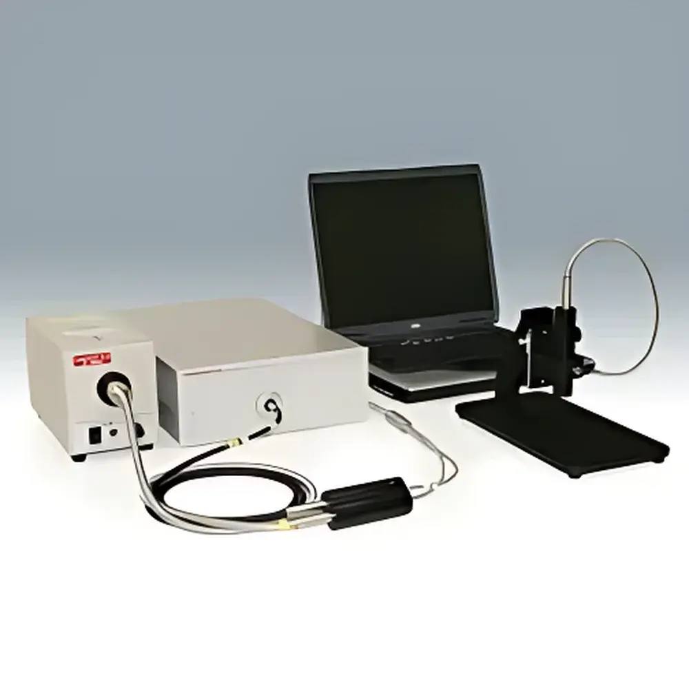
Hamamatsu C10178-01 Optical Spectral Interferometric Thin-Film Thickness Metrology System
| Brand | Hamamatsu |
|---|---|
| Origin | Japan |
| Manufacturer | Hamamatsu Photonics K.K. |
| Type | Imported Instrument |
| Model | C10178-01 |
| Light Source | Halogen Lamp |
| Wavelength Range | 400 nm to 1100 nm |
| Spot Size | Approx. φ1 mm |
| Working Distance | 10 mm |
| Measurable Thickness Range (on Glass Substrate) | 20 nm to 50 µm |
| Thickness Repeatability (SiO₂, 400 nm) | 0.01 nm |
| Thickness Accuracy (on Glass) | ±0.4 % |
| Maximum Detectable Layers | 10 |
| Analysis Methods | FFT-based Interference Analysis, Curve Fitting, Complex Refractive Index (n, k) Modeling |
| Measurement Speed | 19 ms per point (acquisition only) |
| Fiber Interface | φ12 mm Sleeve-Type |
| Communication Interfaces | RS-232C, PIPE, Ethernet, USB 2.0 |
| Power Supply | AC 100–120 V / 200–240 V, 50/60 Hz |
| Power Consumption | 250 W |
Overview
The Hamamatsu C10178-01 Optical Spectral Interferometric Thin-Film Thickness Metrology System is a non-contact, high-resolution metrology platform engineered for precision characterization of thin-film structures using spectral-domain optical coherence interferometry (SD-OCI). Unlike conventional ellipsometers or reflectometers, the C10178-01 leverages broadband spectral interference patterns generated by low-coherence light reflected from multiple interfaces within a layered sample. By analyzing the Fourier-transformed spectral envelope—captured via Hamamatsu’s proprietary Photonic Multichannel Analyzer (PMA)—the system reconstructs optical path differences with sub-nanometer resolution. This principle enables absolute thickness determination without prior knowledge of layer composition, making it especially suitable for process development, QC/QA in semiconductor fabrication, optical coating R&D, and advanced photonic device manufacturing where rapid, traceable, and non-destructive quantification of film stacks is required.
Key Features
- Sub-nanometer repeatability (0.01 nm on SiO₂ reference films) validated under controlled environmental conditions and standardized calibration protocols.
- Real-time point measurement at 19 ms per acquisition—enabling high-throughput mapping across wafers or coated substrates when integrated with motorized XY stages.
- Simultaneous extraction of complex refractive index (n, k) profiles through multi-wavelength fitting algorithms, supporting dispersion modeling for transparent and weakly absorbing layers.
- Multi-layer capability: up to 10 optically distinct interfaces resolved via iterative curve-fitting against physically constrained optical models.
- Modular fiber-coupled architecture with φ12 mm sleeve-type interface, allowing flexible integration into cleanroom tooling, vacuum chambers, or inline production environments.
- Comprehensive optical property quantification beyond thickness: includes normal-incidence reflectance (R), transmittance (T), absorption coefficient (α), and quantum efficiency (QE) when paired with calibrated reference detectors and spectral radiance sources.
Sample Compatibility & Compliance
The C10178-01 accommodates rigid and semi-rigid planar substrates including silicon wafers, fused silica, BK7 glass, sapphire, and ITO-coated substrates. It supports both single-layer and multilayer dielectric, semiconductor, and metallic stack configurations—provided optical contrast exists between adjacent layers and surface roughness remains below λ/10 (i.e., <40 nm RMS for 400 nm light). The system complies with ISO/IEC 17025 requirements for calibration traceability when operated with NIST-traceable reference standards. Measurement uncertainty budgets align with VLSI Standard Measurement Assurance Program (SMP) guidelines, and documentation supports GLP/GMP audit readiness—including full instrument configuration logs, calibration certificate archives, and raw spectral data export in HDF5 or ASCII formats.
Software & Data Management
Control and analysis are executed via Hamamatsu’s dedicated Metrology Suite software, which provides a deterministic, scriptable environment compliant with FDA 21 CFR Part 11 for electronic records and signatures. The suite supports automated stage control, batch measurement scheduling, statistical process control (SPC) charting, and pass/fail thresholding based on user-defined tolerances. All raw interferograms, fitted spectra, and derived parameters are stored with embedded metadata (timestamp, operator ID, environmental sensor readings, optical alignment status). Data export adheres to ASTM E1394 and ISO 10360-7 standards for interoperability with LIMS and MES platforms. Remote operation is enabled via Ethernet-based PIPE protocol or TCP/IP socket interface, permitting integration into factory automation frameworks (SECS/GEM, OPC UA).
Applications
- Semiconductor front-end process monitoring: gate oxide, hard mask, ARC, and low-k dielectric thickness uniformity mapping on 200 mm and 300 mm wafers.
- Optical coating validation: anti-reflection, high-reflection, and bandpass filter stacks on lenses, mirrors, and laser cavity components.
- Photovoltaic R&D: transparent conductive oxide (TCO) layer optimization, perovskite absorber thickness profiling, and interfacial defect detection.
- MEMS/NEMS fabrication: sacrificial layer etch depth verification and residual stress-induced curvature correction.
- Academic thin-film physics: dispersion analysis of novel 2D materials (e.g., MoS₂, h-BN) and plasmonic nanostructures.
FAQ
What optical principles underpin the C10178-01’s thickness measurement capability?
It operates on spectral-domain optical coherence interferometry, resolving layer thicknesses by Fourier analysis of interference fringes generated from broadband halogen illumination (400–1100 nm) reflected across dielectric interfaces.
Can the system measure films on curved or patterned substrates?
Standard operation assumes flat, macroscopically uniform surfaces. Curved substrates require custom objective optics and Z-height compensation; patterned samples may be measured if feature pitch exceeds the 1 mm spot diameter and topography variation remains within depth-of-field limits.
Is calibration required before each measurement session?
No routine recalibration is needed between sessions. However, daily verification using certified SiO₂-on-silicon reference wafers is recommended to maintain traceability per ISO/IEC 17025 Annex A.3.
Does the software support automated report generation for quality audits?
Yes—Metrology Suite includes configurable PDF/CSV report templates with embedded digital signatures, revision history, and compliance flags aligned with ISO 9001 and IATF 16949 documentation requirements.
How is measurement uncertainty quantified and documented?
Uncertainty budgets follow GUM (JCGM 100:2008) methodology and are recorded per measurement point, incorporating contributions from spectral noise, wavelength calibration drift, substrate refractive index uncertainty, and model parameter correlation effects.