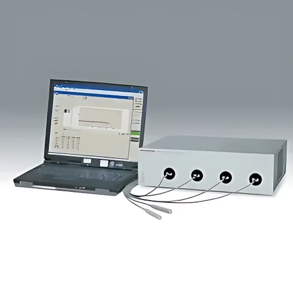
Hamamatsu C11295 Multi-Point Nanometer Thin-Film Thickness Measurement System
| Brand | Hamamatsu |
|---|---|
| Origin | Japan |
| Manufacturer | Hamamatsu Photonics K.K. |
| Type | Imported Instrument |
| Model | C11295 |
| Pricing | Upon Request |
| Measurement Principle | Spectral Coherence Interferometry |
| Max. Measurement Points | 15 |
| Thickness Range (on glass, SiO₂-equivalent) | 20 nm to 100 μm |
| Repeatability (400 nm SiO₂ film) | 0.02 nm (1σ) |
| Accuracy (on glass) | ±0.4 % |
| Wavelength Range | 320 nm – 1000 nm |
| Spot Size | Approx. φ1 mm |
| Working Distance | 10 mm |
| Max. Layers Analyzable | 10 |
| Analysis Methods | FFT-based spectral analysis & optical model fitting |
| Measurement Time per Point | 19 ms (acquisition only) |
| Light Source | Xenon lamp |
| Fiber Interface | SMA |
| External Control Interfaces | Ethernet, USB 2.0 (main unit), RS-232C (light source) |
| Power Supply | AC 100–240 V, 50/60 Hz |
| Power Consumption | ~330 W (2-channel) to ~450 W (15-channel) |
Overview
The Hamamatsu C11295 Multi-Point Nanometer Thin-Film Thickness Measurement System is an engineered solution for in-line and offline metrology in semiconductor process development and high-precision thin-film manufacturing environments. It employs spectral coherence interferometry (SCI), a non-contact, non-destructive optical technique that leverages broadband interference fringes generated by partial coherence of light reflected from multiple dielectric interfaces. Unlike conventional ellipsometry or single-wavelength reflectometry, SCI enables simultaneous extraction of thickness and complex refractive index (n, k) across a wide spectral band—without requiring physical reference samples or prior knowledge of layer stack composition. The system is designed for integration into advanced process tools—including cluster tools with APC (Advanced Process Control) modules—where real-time, spatially resolved metrology supports closed-loop feedback for deposition, etch, and CMP processes.
Key Features
- Simultaneous multi-point measurement at up to 15 discrete locations within a single acquisition cycle, enabling spatial uniformity mapping across wafers or large-area substrates.
- Reference-free operation: eliminates dependency on calibration standards or pre-characterized reference films, reducing setup time and long-term drift sensitivity.
- Integrated photometric stabilization: real-time correction for source intensity fluctuations and environmental thermal drift ensures measurement stability over extended operational periods (>8 hours).
- Concurrent acquisition of spectral reflectance (or transmittance), color coordinates (CIE L*a*b*), and temporal dynamics—supporting both static metrology and process transient monitoring.
- High-speed data capture: 19 ms per point acquisition time (excluding computational fitting), compatible with high-throughput production environments.
- Optical constant extraction: full n(λ) and k(λ) dispersion modeling via physics-based fitting algorithms, supporting characterization of amorphous, polycrystalline, and graded-index films.
- Robust mechanical architecture: optimized for cleanroom compatibility, including vibration-damped optical housing and ESD-safe interface design.
Sample Compatibility & Compliance
The C11295 accommodates a broad range of substrate materials (Si, SiO₂, sapphire, quartz, fused silica, and flexible polymer films) and multilayer stacks—up to 10 optically distinct layers—with no requirement for surface planarity. Its 1-mm spot size and 10-mm working distance enable reliable measurements on patterned wafers, stepped structures, and curved surfaces. The system complies with ISO/IEC 17025 requirements for calibration traceability when used with Hamamatsu-certified reference standards. For regulated environments, the instrument supports audit-ready data logging (timestamped, user-ID tagged, and immutable metadata embedding) aligned with FDA 21 CFR Part 11 principles when paired with validated third-party LIMS or MES platforms. All optical components meet SEMI F20 cleanroom particulate emission specifications.
Software & Data Management
The system operates under Hamamatsu’s proprietary THICKNESS ANALYZER software suite, which provides real-time visualization of spectral interferograms, live thickness maps, and layer-by-layer optical model editing. Raw spectral data (intensity vs. wavelength) and fitted parameters are stored in HDF5 format—ensuring interoperability with MATLAB, Python (h5py), and industry-standard metrology databases. Batch analysis workflows support automated pass/fail classification against user-defined tolerance bands, with configurable alarm triggers (visual, audible, and digital I/O outputs). Software export functions include CSV, XML, and PDF reports compliant with internal QA documentation protocols. Remote operation and firmware updates are supported via secure Ethernet connection using TLS 1.2 encryption.
Applications
- In-situ monitoring of PECVD, ALD, and sputtered dielectric films (SiO₂, SiNₓ, Ta₂O₅, HfO₂) during deposition.
- Post-deposition uniformity verification across 200 mm and 300 mm silicon wafers.
- Characterization of anti-reflective coatings, OLED encapsulation layers, and photovoltaic absorber stacks.
- Quality control of optical filters, MEMS structural layers, and biomedical thin-film sensors.
- Research-grade determination of dispersion-corrected optical constants for novel 2D materials and metamaterials.
- Integration with factory automation systems via SECS/GEM protocol translation gateways (optional).
FAQ
What is the minimum measurable film thickness on silicon substrates?
The practical lower limit is ~20 nm for transparent dielectrics (e.g., SiO₂) on Si; sub-10 nm resolution is achievable for high-contrast stacks (e.g., metal/dielectric) using advanced phase-sensitive fitting.
Can the system measure through opaque substrates?
No—it requires optical access to the film surface; transmission-mode measurement is only supported for transparent or semi-transparent substrates (e.g., glass, quartz, sapphire).
Is GLP/GMP-compliant electronic record keeping supported?
Yes—when deployed with validated software configuration and external audit-trail infrastructure, the system meets ALCOA+ data integrity criteria for regulated laboratories.
How is calibration maintained over time?
The system uses internal reference channels and factory-calibrated spectral response curves; annual recalibration against NIST-traceable thickness standards is recommended per ISO/IEC 17025.
Does it support custom optical models for anisotropic or gradient-index films?
Yes—the fitting engine accepts user-defined dispersion models (Cauchy, Sellmeier, Tauc-Lorentz) and supports graded-layer parameterization via spline interpolation.