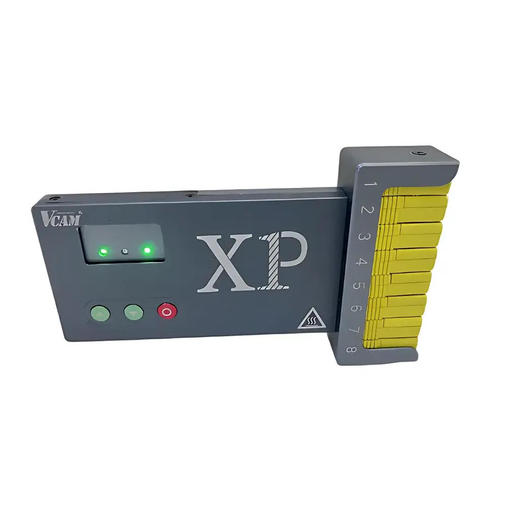
Hamamatsu C11627-01 Optical Thin-Film Thickness Measurement System
| Brand | Hamamatsu |
|---|---|
| Origin | Japan |
| Manufacturer Type | Original Equipment Manufacturer (OEM) |
| Product Category | Imported Instrument |
| Model | C11627-01 |
| Price | Upon Request |
| Measurement Principle | Spectral Interferometry (White-Light Coherence Scanning) |
| Measurable Thickness Range (on Glass Substrate) | 20 nm to 50 µm |
| Repeatability (SiO₂, 400 nm film) | 0.02 nm (1σ) |
| Accuracy (Glass Substrate) | ±0.4 % (per VLSI Standard Calibration Certificate) |
| Light Source | Broadband LED |
| Wavelength Range | 420 nm – 720 nm |
| Spot Size | Approx. Ø1 mm |
| Working Distance | 10 mm |
| Max. Detectable Layers | 10 |
| Analysis Methods | FFT-based Coherence Peak Detection, Least-Squares Curve Fitting, Refractive Index (n) & Extinction Coefficient (k) Extraction |
| Measurement Speed | 19 ms per data point (acquisition only, excluding analysis) |
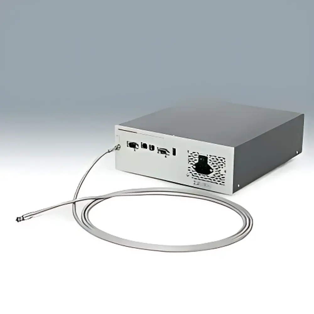
| Fiber Interface | FC-type |
| External Control Interfaces | RS-232C, Ethernet |
| Power Supply | AC 100–240 V, 50/60 Hz |
| Power Consumption | 70 W |
Overview
The Hamamatsu C11627-01 Optical Thin-Film Thickness Measurement System is a compact, non-contact metrology instrument engineered for high-precision, real-time thickness characterization of transparent and semi-transparent thin films on rigid substrates. It operates on the principle of spectral interferometry—specifically, white-light coherence scanning—where broadband interference fringes generated at film-substrate and air-film interfaces are spectrally resolved and analyzed to determine optical path differences. Unlike conventional ellipsometers or stylus profilometers, the C11627-01 requires no reference sample or mechanical referencing step; its absolute measurement capability eliminates drift-induced calibration errors and enables long-term stability in production-line or cleanroom environments. The system integrates a stabilized LED source, miniature spectrometer, and embedded signal processing unit into a single monolithic head, connected to host instrumentation exclusively via a single FC-terminated optical fiber. This architecture minimizes alignment sensitivity, reduces footprint, and supports OEM integration into semiconductor process tools, vacuum deposition chambers, or inline coating monitoring stations.
Key Features
- Reference-free operation: Eliminates need for periodic reference measurements or recalibration against known standards—critical for unattended, 24/7 process monitoring.
- Compact monolithic design: Total system volume < 1.2 L; optimized for space-constrained integration (e.g., behind viewports, within tool-side enclosures).
- High-speed acquisition: 19 ms per spatial point enables rapid mapping across wafers or coated panels without compromising resolution.
- Multi-layer capability: Simultaneous determination of individual layer thicknesses and optical constants (n, k) for up to 10 stacked dielectric or semiconductor films.
- Sub-nanometer repeatability: Achieves 0.02 nm (1σ) thickness repeatability on SiO₂ films under controlled thermal and vibration conditions—validated per ISO 5725-2:2019 guidelines.
- Robust optical interface: FC-connectorized fiber delivery ensures stable coupling across temperature cycles and mechanical perturbations typical in industrial settings.
Sample Compatibility & Compliance
The C11627-01 is validated for use on flat, optically smooth substrates including fused silica, silicon wafers, BK7 glass, and sapphire. It supports measurement of amorphous, polycrystalline, and epitaxial layers such as SiO₂, Si₃N₄, TiO₂, Al₂O₃, ITO, and photoresists—provided surface roughness remains below λ/10 (i.e., < 40 nm RMS for visible wavelengths). The system complies with electromagnetic compatibility requirements per IEC 61326-1:2022 (industrial environment) and meets safety standards under IEC 61010-1:2010. While not certified for GMP or FDA-regulated environments out-of-the-box, its deterministic measurement algorithm, full audit trail logging (via external PC), and RS-232C/Ethernet command protocol support validation per 21 CFR Part 11 when deployed with compliant software infrastructure. Traceable calibration certificates aligned to NIST-traceable VLSI reference standards are provided with each unit.
Software & Data Management
The system operates via Hamamatsu’s proprietary C11627 Control Suite (v3.x), a Windows-based application supporting real-time visualization, batch mapping, and automated report generation in PDF or CSV format. All raw interferogram spectra, fitted models, and metadata—including timestamp, environmental sensor readings (optional), and operator ID—are stored in HDF5 format to ensure long-term readability and interoperability with MATLAB, Python (h5py), or LabVIEW. The Ethernet interface enables remote configuration, triggering, and data streaming at up to 50 Hz sustained rate—facilitating synchronization with motion stages or PLC-controlled processes. For integration into MES or SCADA platforms, a documented ASCII command set (SCPI-compatible syntax) and TCP/IP socket API are supplied, enabling full control without proprietary drivers.
Applications
- Semiconductor front-end process control: Monitoring PECVD, ALD, and sputtered dielectric stacks during wafer fabrication.
- Optical coating QC: Thickness verification of anti-reflective, high-reflection, and filter coatings on lenses and laser components.
- MEMS and display manufacturing: In-situ thickness tracking of sacrificial layers, passivation films, and OLED encapsulation barriers.
- R&D laboratories: Quantitative n/k dispersion modeling for novel 2D materials (e.g., MoS₂, h-BN) and perovskite thin films.
- Photovoltaics: Inline measurement of TCO (ITO, AZO) and absorber layer uniformity on large-area glass substrates.
FAQ
Does the C11627-01 require periodic recalibration using reference standards?
No. Its self-referencing coherence peak detection algorithm eliminates dependence on physical reference samples. However, annual verification using Hamamatsu-supplied NIST-traceable VLSI calibration wafers is recommended for compliance-critical applications.
Can it measure films on curved or textured substrates?
It is designed for planar, low-scatter surfaces. Curved substrates introduce defocus and beam distortion; surface roughness > 40 nm RMS degrades fringe contrast and fitting confidence. Optional telecentric objectives (sold separately) extend working distance and improve tolerance for mild curvature.
Is the 19 ms measurement time achievable during continuous raster scanning?
Yes—provided the host controller buffers triggers and manages stage motion latency. Full spectral acquisition occurs at 52 Hz; post-processing time depends on layer model complexity but is typically < 50 ms per point on modern x64 systems.
What optical constants databases are included?
The software ships with built-in Cauchy, Sellmeier, and Tauc-Lorentz dispersion models. Users may import custom n/k datasets from ellipsometry or spectroscopic reflectometry sources in tab-delimited format.
How is thermal drift mitigated during extended measurements?
The LED source and spectrometer are thermally stabilized to ±0.1 °C. Internal temperature sensors log thermal transients, and optional ambient temperature compensation algorithms adjust thickness output based on real-time substrate expansion coefficients.