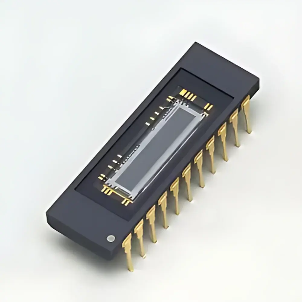
Hamamatsu CMOS Linear Image Sensor S10121-256Q-01
| Brand | Hamamatsu |
|---|---|
| Origin | Japan |
| Manufacturer Type | Original Equipment Manufacturer (OEM) |
| Product Category | Imported Optical Component |
| Model | S10121-256Q-01 |
| Component Type | Optical Element |
| Image Area | 12.8 × 2.5 mm |
| Effective Pixels | 256 × 1 |
| Pixel Pitch | 50 µm |
| Pixel Size | 50 × 2500 µm |
| Spectral Response Range | 200–1000 nm |
| Typical Line Rate | 969 lines/s |
| Cooling | Non-cooled |
| Window Material | Quartz |
| Package | Ceramic |
| Recommended Driver ICs | C10808 / C10808-01 |
| Saturation Charge (Typ.) | 140 pC |
| Operating Conditions | Ta = 25 °C, Vdd = 5 V, Vb = Vofd = 2 V, Vofg = 0.2 V, f(CLK) = 200 kHz |
Overview
The Hamamatsu CMOS Linear Image Sensor S10121-256Q-01 is a high-performance, self-scanning photodiode array engineered for precision spectral detection in compact and benchtop optical spectrometers. Designed with a monolithic CMOS architecture, it operates on a current-output principle with programmable per-pixel integration time—enabling dynamic range optimization across varying illumination intensities without external gain staging. Its 256-pixel linear configuration delivers spatial resolution of 50 µm pitch over a 12.8 mm active length, paired with an unusually tall photosensitive height of 2.5 mm to maximize photon collection efficiency—particularly critical in low-flux UV-VIS applications. The sensor exhibits flat quantum efficiency from 200 nm to 350 nm, achieved through a fused silica (quartz) window and optimized anti-reflection coating, minimizing spectral distortion in demanding ultraviolet spectroscopy workflows such as ozone monitoring, UV curing validation, or semiconductor process control.
Key Features
- Programmable per-pixel integration time: Enables real-time exposure adaptation for heterogeneous spectral irradiance profiles—essential for broadband light sources with strong UV/VIS/NIR intensity gradients.
- UV-enhanced responsivity: Peak quantum efficiency >65% at 254 nm; <±3% spectral non-uniformity across 200–350 nm band under calibrated illumination.
- Large-area pixels: 50 µm × 2500 µm pixel geometry improves signal-to-noise ratio (SNR) by increasing full-well capacity while maintaining spatial sampling fidelity required for diffraction-limited grating-based systems.
- Low-power self-scanning operation: Integrated shift register and timing logic reduce system-level driver complexity; compatible with Hamamatsu’s dedicated C10808/C10808-01 clock driver ICs for jitter-free line synchronization.
- Ceramic hermetic package with quartz window: Ensures long-term stability in ambient laboratory environments and resistance to humidity-induced spectral drift—critical for GLP-compliant calibration traceability.
Sample Compatibility & Compliance
The S10121-256Q-01 is designed for integration into OEM optical instruments where detector linearity, spectral fidelity, and thermal stability are governed by international standards. It supports compliance-ready system architectures adhering to ISO/IEC 17025 requirements for measurement uncertainty estimation, particularly when used with NIST-traceable deuterium/halogen lamp calibration sources. Its non-cooled operation meets IEC 61000-4-2 (ESD immunity) and IEC 61326-1 (EMC for laboratory equipment) specifications when implemented with proper PCB layout practices (e.g., guard traces, ground plane continuity). While not certified as a standalone medical device, the sensor is routinely deployed in FDA 21 CFR Part 11–aligned UV-Vis analyzers when embedded within validated instrument firmware that implements audit trails, electronic signatures, and data integrity controls.
Software & Data Management
Hamamatsu provides comprehensive SDK support—including C/C++ libraries, LabVIEW VIs, and Python bindings—for seamless integration into spectral acquisition platforms. Raw analog output is digitized via external 16-bit ADCs (e.g., ADS8860), with timing signals synchronized to the sensor’s CLK, SH, and RS pins. The SDK enables pixel-level dark offset correction, non-uniformity compensation (NUC), and real-time line-rate adjustment—facilitating adaptive acquisition strategies such as multi-integration scanning (MIS) for extended dynamic range. Exported spectra conform to ASTM E131-22 (Standard Terminology Relating to Molecular Spectroscopy) metadata conventions, supporting interoperability with Thermo Fisher OMNIC, Ocean Insight SpectraSuite, and open-source tools like PySpectra and SpecUtils.
Applications
- Compact UV-Vis spectrometers for environmental monitoring (e.g., NO₂, SO₂, O₃ absorption spectroscopy in open-path or gas-cell configurations).
- Process analytical technology (PAT) systems in pharmaceutical manufacturing—real-time monitoring of UV-active excipients during wet granulation or film coating.
- UV LED spectral characterization in R&D labs, including peak wavelength, FWHM, and radiant flux quantification per IES LM-79.
- Miniaturized Raman spectrometers utilizing 254/365 nm excitation, leveraging the sensor’s low etaloning and high UV QE.
- Educational optics platforms requiring robust, low-threshold detectors for Fourier-transform or grating-based experiments under undergraduate laboratory conditions.
FAQ
What is the recommended driving circuit for optimal line rate stability?
The C10808 or C10808-01 clock driver IC is specified to minimize clock skew and ensure <±0.5% line-rate variation across temperature (−10 to +60 °C).
Can this sensor be used in vacuum or controlled-atmosphere enclosures?
Yes—the ceramic package with quartz window maintains hermeticity up to 1×10⁻⁴ Pa; however, outgassing of internal bond wires must be assessed per ASTM E595 for space-grade applications.
Does Hamamatsu provide radiometric calibration data for individual units?
Yes—NIST-traceable relative spectral responsivity (RSR) curves and pixel-to-pixel uniformity reports are available as optional add-ons (Order Code: CAL-S10121-256Q-01).
How does saturation charge translate to maximum irradiance handling?
At 200 nm and 10 ms integration time, the 140 pC saturation limit corresponds to ~1.2 µW/mm² irradiance on the active area—calculated using standard photoelectron yield models for silicon photodiodes.
Is there a pin-compatible upgrade path to higher-resolution variants?
The S10121-512Q-01 (512-pixel version) shares identical footprint, timing protocol, and drive requirements—enabling drop-in resolution scaling without PCB redesign.


