Hamamatsu FOS Series CsI(Tl) Scintillator Screens
| Brand | Hamamatsu |
|---|---|
| Origin | Japan |
| Manufacturer Type | Original Equipment Manufacturer (OEM) |
| Import Status | Imported |
| Model | FOS Series |
| Pricing | Available Upon Request |
| Scintillator Material | Thallium-doped Cesium Iodide (CsI:Tl) |
| Substrate | Fiber Optic Plate (FOP) |
| Standard Thickness | 150 µm |
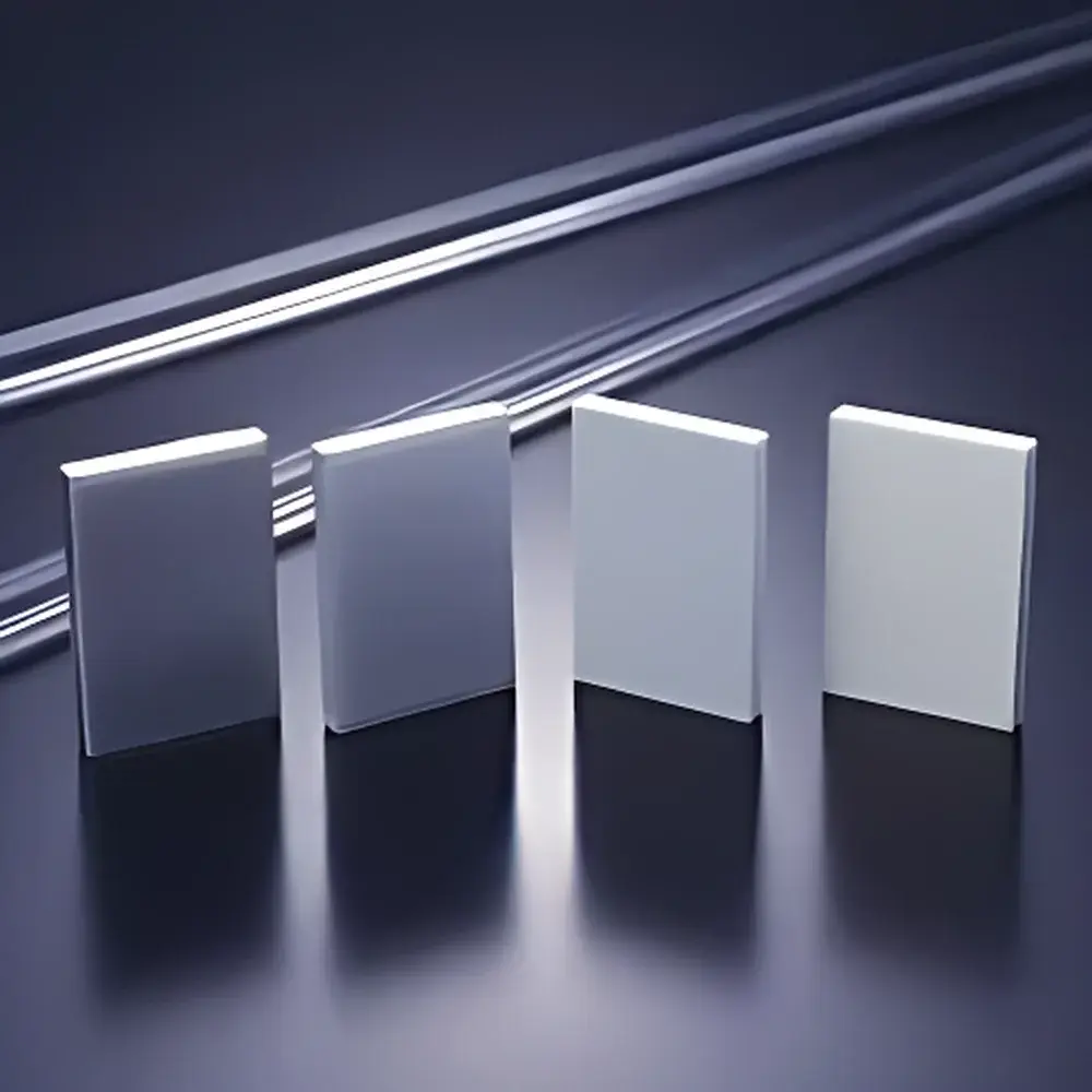
| Available Formats | Rectangular and Circular Configurations |
| Effective Area Range | 15 × 15 mm to 47 × 47 mm |
| Optical Coupling | Direct fiber-optic coupling to CCD/CMOS sensors |
| Spectral Emission Peak | ~550 nm (matches silicon-based detector quantum efficiency) |
Overview
The Hamamatsu FOS Series CsI(Tl) scintillator screens are high-performance, fiber-optic-plate (FOP)-bonded X-ray conversion devices engineered for high-resolution indirect detection in digital radiography systems. These screens utilize thallium-doped cesium iodide (CsI:Tl) as the scintillating material—a crystalline phosphor known for its high X-ray absorption coefficient (especially in the 20–120 kVp diagnostic range), columnar microstructure that minimizes lateral light spread, and strong green emission peaking at approximately 550 nm—optimal for spectral matching with back-illuminated CCD and scientific CMOS sensors. Unlike powdered or polycrystalline scintillators, the vapor-deposited columnar CsI:Tl layer on fused silica FOP substrates ensures intrinsic spatial resolution preservation, reduced afterglow (65% optical throughput at 550 nm) without requiring external optical coupling gels or adhesives—critical for reproducible, maintenance-free integration into OEM imaging subsystems.
Key Features
- Fiber-optic plate (FOP) substrate with direct CsI:Tl vapor deposition—eliminates interfacial losses and delamination risk
- Uniform 150 µm columnar CsI:Tl thickness across all standard configurations—ensures consistent detective quantum efficiency (DQE) and modulation transfer function (MTF)
- Multiple active area options: rectangular formats (15 × 15 mm to 47 × 47 mm effective area) and circular variants (Ø23.5 mm) to match common sensor footprints
- High X-ray absorption: >85% at 40 kVp (Al filtration), >65% at 80 kVp—enabling low-dose operation in dental, mammographic, and NDT applications
- Low afterglow and fast decay time (primary component τ ≈ 1 µs; slow component <1% at 10 ms)—supports real-time fluoroscopic frame rates up to 30 fps
- OEM-ready design: No electrical connections or power requirements; compatible with vacuum-sealed or inert-gas-filled detector housings
Sample Compatibility & Compliance
The FOS series is designed for integration into regulated X-ray imaging platforms compliant with international safety and performance standards. Its CsI:Tl composition meets ISO 15708-2:2017 (non-destructive testing—characterization of industrial X-ray systems) requirements for scintillator linearity and dose response. The hermetically sealed FOP structure satisfies IEC 62220-1-2:2019 (digital X-ray detectors—part 1-2: characteristics and test methods for fluoroscopic systems) environmental robustness criteria, including resistance to thermal cycling (−10°C to +50°C) and humidity exposure (up to 95% RH non-condensing). While not a standalone medical device, the screen conforms to essential principles of ISO 13485:2016 when incorporated into Class IIa/IIb medical imaging subsystems, and supports traceable calibration workflows required under FDA 21 CFR Part 820 and EU MDR Annex II.
Software & Data Management
As a passive optical component, the FOS screen requires no embedded firmware or driver software. Its performance is characterized via standardized metrology protocols—including MTF measurement using edge-spread function (ESF) analysis, DQE calculation per IEC 62220-1-1, and absolute sensitivity calibration using traceable X-ray reference beams (e.g., NIST SRM 2082). Hamamatsu provides comprehensive technical documentation (including spectral responsivity curves, light output vs. dose curves, and angular dependence data) in machine-readable formats (CSV, PDF) for integration into OEM quality management systems. All units ship with individual serial-numbered calibration certificates aligned to JIS Z 4901:2018 (radiation detection instrumentation—calibration of scintillation detectors).
Applications
- Dental intraoral and panoramic radiography systems requiring sub-50 µm effective pixel pitch
- Mammography detectors operating in the 25–35 kVp range, where CsI:Tl’s high K-edge absorption (33.2 keV) maximizes contrast-to-noise ratio
- Industrial computed radiography (CR) and real-time radiography (RTR) for aerospace and automotive NDT
- Micro-CT preclinical imaging systems with high magnification optics and low-noise sCMOS readout
- Beamline diagnostics in synchrotron facilities—compatible with pulsed X-ray sources and time-resolved acquisition
FAQ
What is the typical light output of the FOS screen per unit X-ray dose?
The nominal light yield is 55–60 photons per keV of absorbed X-ray energy, measured under 40 kVp W/Al beam conditions with calibrated photodiode reference.
Can the FOS screen be used with CMOS sensors?
Yes—its 550 nm emission peak aligns closely with peak quantum efficiency of modern back-thinned scientific CMOS sensors (e.g., sCMOS with >80% QE at 550 nm).
Is the CsI:Tl layer hygroscopic? How is moisture protection ensured?
CsI:Tl is inherently hygroscopic, but the monolithic FOP bonding process fully encapsulates the scintillator layer, eliminating exposure to ambient humidity—even during prolonged storage or operation in non-controlled environments.
Does Hamamatsu provide custom dimensions or thicknesses?
Standard offerings are fixed at 150 µm thickness; custom thicknesses (e.g., 100 µm for higher resolution or 200 µm for increased sensitivity) and non-standard geometries are available under OEM agreement with minimum order quantities.
How is spatial uniformity verified across the active area?
Each production lot undergoes full-field flat-field illumination testing using a stabilized LED source at 550 nm; pixel-to-pixel response variation is guaranteed ≤±3.5% over the effective area (per Hamamatsu QA-127 specification).


