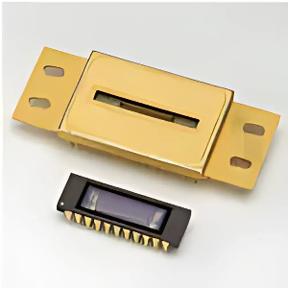
Hamamatsu InGaAs Linear and Area Array Image Sensors for SWIR Hyperspectral Imaging
| Origin | Japan |
|---|---|
| Manufacturer Type | Authorized Distributor |
| Import Status | Imported |
| Model Series | InGaAs |
| Frame Rate | 1031 fps (area array) to 7200 lines/s (linear array) |
| Spectral Range | 900–2550 nm |
| Spectral Response | SWIR (Short-Wave Infrared) |
| Cooling | Uncooled, Single-Stage TE, or Dual-Stage TE |
| Pixel Pitch | 25–50 µm |
| Pixel Count | 256–16384 |
| Active Area | 3.2 × 3.2 mm to 25.6 × 0.5 mm |
| Optical Interface | Binary optical element compatible |
| Platform Compatibility | Ground-based and airborne hyperspectral systems |
| Compliance | RoHS-compliant packaging, ISO 9001-certified manufacturing environment |
Overview
Hamamatsu InGaAs linear and area array image sensors are solid-state photodetectors engineered for high-sensitivity detection in the short-wave infrared (SWIR) spectral region (900–2550 nm). Based on indium gallium arsenide (In0.53Ga0.47As) lattice-matched to InP substrates, these sensors operate via photovoltaic conversion under reverse bias, delivering low dark current, high quantum efficiency (>70% across 1000–1700 nm), and excellent linearity over six orders of magnitude. Unlike thermal detectors, InGaAs sensors provide photon-counting capability at room temperature (uncooled variants) or enhanced signal-to-noise ratio (SNR) with thermoelectric (TE) cooling—making them ideal for time-resolved spectroscopy, rapid-scanning hyperspectral imaging, and low-light analytical applications where spectral fidelity and temporal resolution are critical. These devices serve as the core optoelectronic transducer in push-broom and snapshot hyperspectral systems used in laboratory, industrial, and remote sensing platforms.
Key Features
- SWIR-optimized spectral response spanning 900–2550 nm, with model-specific cutoffs (e.g., G9205-256W: 1850 nm; G9208-256W: 2550 nm)
- Multiple architecture options: high-speed linear arrays (up to 7200 lines/s) and TE-cooled area arrays (up to 1031 fps at 64 × 64 format)
- Pixel pitches from 25 µm to 50 µm, supporting spatial sampling trade-offs between resolution and sensitivity
- Integrated on-chip analog signal conditioning—including correlated double sampling (CDS) in select models—to suppress reset noise and improve dynamic range
- Robust hermetic packaging with AR-coated windows optimized for 1000–1700 nm transmission
- Compliance with JEDEC JESD22-A108 reliability standards for temperature cycling and humidity exposure
Sample Compatibility & Compliance
These InGaAs sensors are designed for integration into spectrometers, hyperspectral imagers, and OEM analytical modules compliant with international instrumentation standards. Their spectral response aligns with ASTM E131-22 (Standard Terminology Relating to Molecular Spectroscopy) and supports measurement traceability per ISO/IEC 17025:2017 for calibration laboratories. For regulated environments—including pharmaceutical QC and environmental monitoring—the TE-cooled variants (e.g., G9205–G9208 series) support GLP-compliant data acquisition when paired with validated firmware and audit-trail-capable host software. All units meet RoHS Directive 2011/65/EU requirements for hazardous substances and are manufactured in Hamamatsu’s ISO 9001-certified facilities in Japan.
Software & Data Management
Hamamatsu provides SDKs (C/C++, Python, LabVIEW) enabling full control of exposure timing, gain, offset, and readout mode. Raw frame/line data output is delivered in IEEE 754-compliant 16-bit unsigned integer format, facilitating direct ingestion into hyperspectral processing pipelines (e.g., ENVI, MATLAB Hypercube Toolbox, or custom Python-based PCA/MNF workflows). Time-stamped metadata—including sensor temperature, bias voltage, and frame counter—is embedded in each acquisition header, satisfying FDA 21 CFR Part 11 requirements for electronic records when deployed with validated host systems. Optional hardware synchronization (TTL trigger input/output) ensures precise alignment with scanning mirrors, laser pulses, or external spectrometer gratings.
Applications
- Industrial sorting: Real-time grain, plastic, and pharmaceutical tablet inspection using spectral reflectance signatures in the 1000–1700 nm window
- Environmental remote sensing: Airborne mapping of vegetation water content (NDWI), soil moisture, and hydrocarbon contamination via SWIR absorption features
- Biomedical research: Time-resolved fluorescence lifetime imaging (FLIM) of NIR-II fluorophores (e.g., IR-26, CH1055)
- Nuclear and high-energy physics: Scintillation light detection in LaBr3:Ce and CeBr3 crystals emitting above 900 nm
- Process analytical technology (PAT): In-line monitoring of chemical reactions involving C–H, O–H, and N–H bond vibrations
- Quantum optics: Single-photon detection in quantum communication channels operating at 1310/1550 nm telecom wavelengths
FAQ
What is the typical dark current specification for uncooled InGaAs linear arrays at room temperature?
Uncooled devices (e.g., G9494 series) exhibit dark current densities below 5 nA/mm² at 25°C, enabling integration times up to 10 ms without significant shot-noise dominance.
Can these sensors be integrated into vacuum-compatible optical systems?
Yes—hermetically sealed ceramic packages with Kovar leads meet UHV outgassing limits per ASTM E595, provided AR coatings are specified for vacuum durability.
Is pixel binning supported in area array models like G11097-0707S?
Hardware binning is not implemented on-chip; however, programmable ROI readout and on-host software binning (2×2, 4×4) are fully supported via the SDK.
How does TE cooling affect spectral responsivity stability?
Single-stage TE stabilization maintains junction temperature within ±0.1°C, reducing responsivity drift to <0.02%/°C across the 900–1700 nm band.
Are evaluation kits available for system prototyping?
Yes—Hamamatsu offers EVK-01 development platforms including FPGA-based digitizers, calibrated reference sources, and spectral calibration certificates traceable to NIST SRM 2035.
Related Products

")