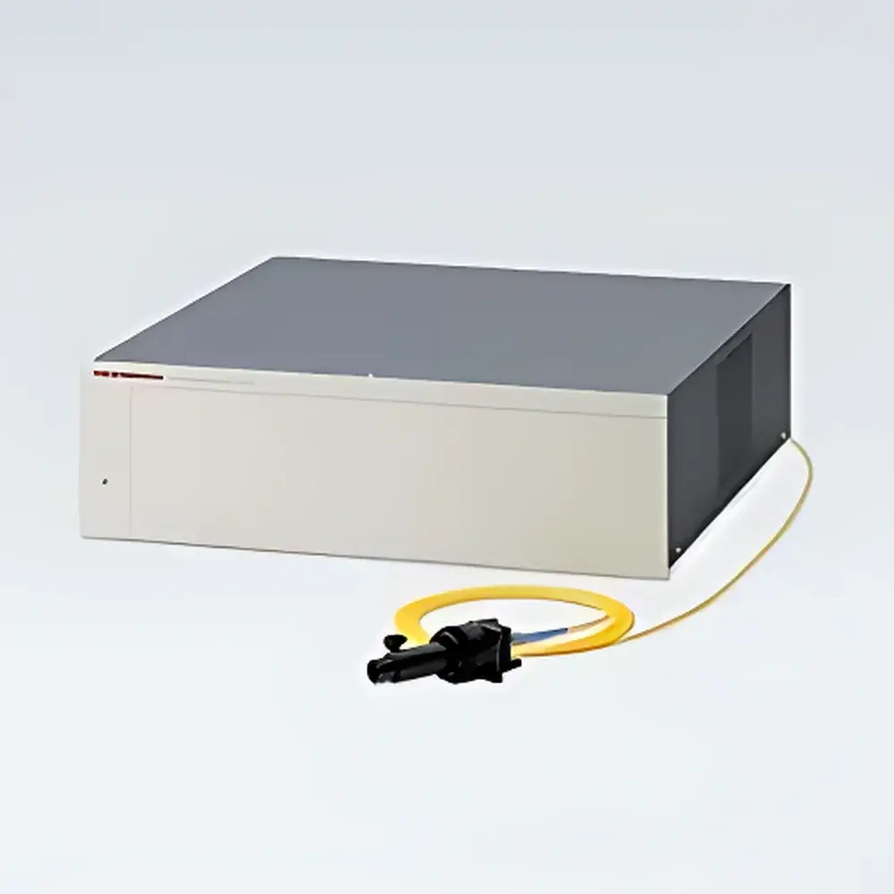
Hamamatsu Optical MicroGauge Thin-Film Thickness Measurement System C11011 Series
| Brand | Hamamatsu |
|---|---|
| Origin | Japan |
| Manufacturer Type | Original Equipment Manufacturer (OEM) |
| Product Category | Imported Instrumentation |
| Model | C11011 Series |
| Pricing | Available Upon Request |
| Measurement Principle | Laser Interferometry (Infrared, 1300 nm) |
| Max. Measurement Speed | 60 Hz |
| Spot Size | ≈ Ø60 µm |
| Working Distance | 155 mm (standard), optional 1000 mm |
| Thickness Range (Glass) | 25 µm – 2.9 mm |
| Thickness Range (Silicon) | 10 µm – 1.2 mm |
| Repeatability (Glass) | ±250 nm |
| Repeatability (Silicon) | ±100 nm |
| Accuracy (Silicon) | ±0.5 µm (≤500 µm), ±0.1% (>500 µm) |
| Max. Layers Measurable | 10 |
| Interface Options | RS-232C, Ethernet, USB 2.0, PIP (Hamamatsu Proprietary Interface Protocol) |
| Power Supply | AC 100–240 V, 50/60 Hz |
| Power Consumption | ~50 VA |
Overview
The Hamamatsu Optical MicroGauge Thin-Film Thickness Measurement System C11011 Series is a non-contact, high-speed interferometric metrology platform engineered for in-line and laboratory-based thickness characterization of optical thin films on semiconductor wafers, glass substrates, and other optically transparent or semi-transparent materials. Operating at a fixed infrared wavelength of 1300 nm, the system leverages low-coherence laser interferometry to resolve film thickness through analysis of interference fringes generated at layer interfaces. Unlike spectral reflectance or ellipsometric methods, this technique delivers robust performance on patterned wafers, surfaces covered with protective films, and non-ideal substrates—including white or diffusely scattering materials—by minimizing sensitivity to surface roughness and ambient light interference. With measurement cycle times as short as 16.7 ms per point and a sustained acquisition rate of up to 60 Hz, the C11011 series supports real-time process monitoring in front-end semiconductor fabrication, photomask inspection, and advanced packaging lines where throughput and temporal resolution are critical.
Key Features
- Non-contact, non-destructive measurement using infrared laser interferometry (1300 nm) optimized for silicon and fused silica substrates
- High-speed point measurement: 16.7–22.2 ms per data point; continuous 60 Hz operation enables dynamic thickness tracking during spin-coating, CVD, or etch processes
- Long working distance (155 mm standard; optional 1000 mm variant available) facilitates integration into cleanroom tools, load-lock chambers, and automated wafer handlers without mechanical interference
- Robust performance on structured surfaces: validated for patterned wafers (e.g., STI, trench arrays) and substrates with temporary protective films (e.g., DUV resists, hard masks)
- Multi-layer capability: models C11011-22 and C11011-22W support up to 10 discrete layer thickness calculations via peak-detection algorithm applied to interferogram envelopes
- Standardized optical interface: FC-type fiber connector ensures compatibility with Hamamatsu’s family of light sources, detectors, and synchronization modules
- Modular external control architecture supporting RS-232C, Ethernet (TCP/IP), USB 2.0 host connection, and Hamamatsu’s proprietary PIP protocol for OEM tool integration
Sample Compatibility & Compliance
The C11011 series is specifically calibrated for industrial semiconductor applications involving silicon (n ≈ 3.67 @ 1300 nm) and optical glass (n ≈ 1.5). Its infrared illumination minimizes absorption in silicon substrates while enabling reliable measurement of oxide, nitride, poly-Si, and photoresist layers ranging from 10 µm to 1.2 mm on Si, and 25 µm to 2.9 mm on glass. The system meets functional requirements aligned with SEMI E10 (Specification for Definition and Measurement of Equipment Reliability, Maintainability, and Availability) and supports traceable calibration procedures compliant with ISO/IEC 17025 principles. While not certified as a medical device or safety-critical instrument, its design adheres to IEC 61000-6-3 (EMC emission limits) and IEC 61000-6-2 (immunity requirements) for industrial environments. Data integrity features—including timestamped raw interferogram logging and configurable audit trails—support alignment with GLP and GMP documentation workflows when integrated with validated LIMS or MES platforms.
Software & Data Management
Hamamatsu provides the dedicated MicroGauge Control Software (v3.x), a Windows-based application supporting real-time visualization, multi-point mapping, statistical process control (SPC) charting, and batch report generation in PDF or CSV format. The software implements deterministic peak-detection algorithms optimized for both single- and multi-layer interferograms, with user-adjustable confidence thresholds and noise filtering parameters. All measurement data—including raw intensity vs. optical path difference (OPD) traces, calculated thickness values, and metadata (timestamp, XY position, environmental sensor readings)—are stored in an open HDF5 container format, enabling third-party analysis in Python (h5py), MATLAB, or JMP. For factory automation, the system exposes a documented COM API and TCP/IP command set compliant with SECS/GEM standards, permitting bidirectional communication with host equipment controllers and enabling closed-loop feedback to deposition tools.
Applications
- Real-time monitoring of spin-on-glass (SOG), BPSG, and TEOS oxide thickness during furnace or PECVD processes
- Post-CMP thickness uniformity assessment across 200 mm and 300 mm wafers
- Quality assurance of anti-reflective coatings on photomasks and reticles
- In-process verification of polymer film thickness in advanced packaging (e.g., redistribution layers, underfill encapsulants)
- R&D characterization of multilayer dielectric stacks for MEMS, photonics, and power devices
- Thickness mapping of curved or warped substrates using optional motorized XYZ stages and auto-focus routines
FAQ
What substrates and film types are supported?
The system is validated for silicon, fused silica, quartz, and borosilicate glass substrates. Compatible films include SiO₂, Si₃N₄, PSG, BPSG, polyimide, SU-8, and most UV-curable resins. Metallic or highly absorbing layers (e.g., Al, Cu) require prior validation due to reduced fringe contrast.
Can it measure through protective films or photoresist layers?
Yes—its 1300 nm wavelength penetrates standard DUV and KrF resist layers up to ~5 µm thick without significant signal attenuation, enabling measurement of underlying oxide or nitride layers without resist removal.
Is the system compatible with cleanroom automation protocols?
Yes. It supports SECS/GEM-compliant messaging over Ethernet and integrates with standard 300 mm FOUP handling systems via RS-232C or PIP-triggered start/stop commands.
How is calibration maintained in production environments?
Hamamatsu supplies NIST-traceable reference wafers with certified thickness steps (SiO₂ on Si). Daily verification follows a two-point check protocol (zero-thickness and mid-range step), with drift correction applied via software offset adjustment.
What is the minimum measurable thickness on silicon?
The practical lower limit is ~10 µm, constrained by coherence length and signal-to-noise ratio—not by optical resolution. Sub-micron films require alternative techniques such as spectroscopic ellipsometry or XRR.


