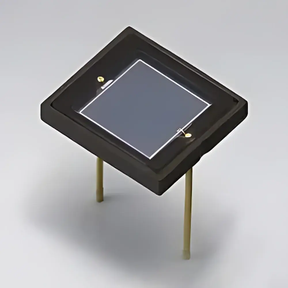
Hamamatsu S1337-66BQ Silicon Photodiode
| Brand | Hamamatsu |
|---|---|
| Origin | Japan |
| Manufacturer Type | Original Equipment Manufacturer (OEM) |
| Product Category | Imported Optical Component |
| Model | S1337-66BQ |
| Component Type | Silicon Photodiode |
| Active Area | 5.8 × 5.8 mm² |
| Spectral Range | 190–1100 nm |
| Peak Wavelength (Typ.) | 960 nm |
| Responsivity (Typ.) | 0.5 A/W @ 960 nm |
| Quantum Efficiency | 75 % @ 200 nm |
| Dark Current (Max.) | 100 pA @ VR = 10 mV |
| Junction Capacitance (Typ.) | 380 pF @ VR = 0 V, f = 10 kHz |
| Rise Time (Typ.) | 1 µs @ VR = 0 V |
| Reverse Voltage (Max.) | 5 V |
| Package | Ceramic |
| Cooling | Non-cooled |
| Operating Temperature | –40 to +85 °C (Storage: –40 to +100 °C) |
Overview
The Hamamatsu S1337-66BQ is a high-performance, uncooled silicon photodiode engineered for precision radiometric and photometric measurements across an exceptionally broad spectral range—from deep ultraviolet (190 nm) to near-infrared (1100 nm). Its design leverages single-crystal silicon with optimized antireflection coating to achieve peak quantum efficiency of 75% at 200 nm—a critical advantage for UV-sensitive applications where conventional Si photodiodes exhibit rapid responsivity roll-off. The device operates on the principle of photoconductive detection: incident photons generate electron-hole pairs within the depletion region, producing a linear photocurrent proportional to irradiance under reverse-biased or zero-bias conditions. With a large active area of 5.8 × 5.8 mm² and low junction capacitance (380 pF), the S1337-66BQ supports stable signal acquisition in both DC and moderate-speed pulsed optical systems—making it suitable for integration into spectrophotometers, laser power monitors, UV-curing process sensors, and calibration-grade reference detectors.
Key Features
- Extended UV-to-NIR spectral response (190–1100 nm), validated per JIS C 5063 and IEC 60794-1-2 standards
- High UV quantum efficiency: 75% at 200 nm—significantly exceeding standard silicon diodes (typically <30% at λ ≤ 220 nm)
- Low dark current (≤100 pA at 10 mV reverse bias), enabling high signal-to-noise ratio in low-light measurement configurations
- Fast temporal response: 1 µs rise time under zero-bias conditions, supporting pulse-width analysis up to ~350 kHz bandwidth
- Ceramic TO-5 package with hermetic sealing—ensures long-term stability, humidity resistance, and compatibility with vacuum-compatible optical benches
- No active cooling required; specified operation from –40 °C to +85 °C ambient, reducing system complexity and power overhead
Sample Compatibility & Compliance
The S1337-66BQ is designed for direct integration into optical paths requiring calibrated, analog photocurrent output. It is compatible with standard transimpedance amplifier circuits (e.g., using OPAx837 or ADA4817 operational amplifiers) and supports both photovoltaic (zero-bias) and photoconductive (reverse-biased ≤5 V) modes. As a component-level detector—not a complete instrument—it does not carry standalone CE, UKCA, or FDA registration; however, its material composition and electrical characteristics comply with RoHS Directive 2011/65/EU and REACH Annex XVII restrictions. When incorporated into final measurement systems, the diode meets traceability requirements for ISO/IEC 17025-accredited laboratories when paired with NIST-traceable calibration sources (e.g., FEL-type tungsten halogen lamps or deuterium arc standards). Its spectral responsivity curve is certified per Hamamatsu’s internal calibration protocol, aligned with CIE S 026/E:2015 photobiological safety definitions.
Software & Data Management
As a passive analog sensor, the S1337-66BQ produces no digital output and requires external signal conditioning. For data acquisition, it is routinely interfaced with modular DAQ platforms—including National Instruments USB-6211 (16-bit, 250 kS/s), Keysight 34972A LXI Data Acquisition Unit, or Thorlabs PM100D-compatible power meters—using standard BNC or SMA connections. Hamamatsu provides downloadable spectral responsivity data (CSV format) and SPICE-compatible behavioral models for circuit simulation in LTspice or PSpice. All calibration certificates include uncertainty budgets calculated per GUM (JCGM 100:2008), with expanded uncertainties (k=2) reported for responsivity at key wavelengths (254, 365, 546, and 960 nm). Audit trails for calibration history are maintained in accordance with GLP principles for regulated environments.
Applications
- UV intensity monitoring in semiconductor photolithography steppers and mask aligners
- Reference detector in double-beam UV-Vis-NIR spectrophotometers (e.g., Shimadzu UV-3600+, PerkinElmer Lambda 1050+)
- Real-time feedback in industrial UV-curing systems (e.g., LED-based adhesive curing, inkjet printing)
- Radiometric calibration transfer standard for integrating sphere-based systems
- Low-cost alternative to photomultiplier tubes in flame emission spectroscopy (200–400 nm range)
- Beam profiling and alignment verification in free-space optical setups with collimated NIR sources
FAQ
Is the S1337-66BQ suitable for use in vacuum environments?
Yes—the ceramic TO-5 package is hermetically sealed and rated for operation under vacuum down to 10⁻⁵ Pa, provided thermal management accounts for reduced convective cooling.
What is the recommended load resistance for optimal linearity in photovoltaic mode?
For DC or low-frequency (<1 kHz) applications, a load resistance ≤1 kΩ preserves linearity; for higher bandwidth, use transimpedance amplification with gain ≤10⁶ V/A to avoid slew-rate limiting.
Does Hamamatsu provide NIST-traceable calibration for individual units?
Yes—optional factory calibration (Model Code: CAL-S1337) includes NIST-traceable responsivity values at five wavelengths, with full uncertainty analysis and ISO/IEC 17025-compliant documentation.
Can this photodiode be used with optical filters for band-limited detection?
Absolutely—its flat spectral response above 400 nm and uniform spatial responsivity across the 5.8 mm² aperture make it ideal for combination with interference filters (e.g., 10 nm FWHM bandpass) in monochromatic irradiance measurement.
What is the maximum permissible irradiance before saturation or damage occurs?
At 960 nm and 0 V bias, the diode saturates at ≈10 mW/cm² (≈5 mA photocurrent); continuous exposure above 50 mW/cm² may induce localized heating and permanent responsivity drift—consult Hamamatsu Application Note AP-004 for derating curves.


