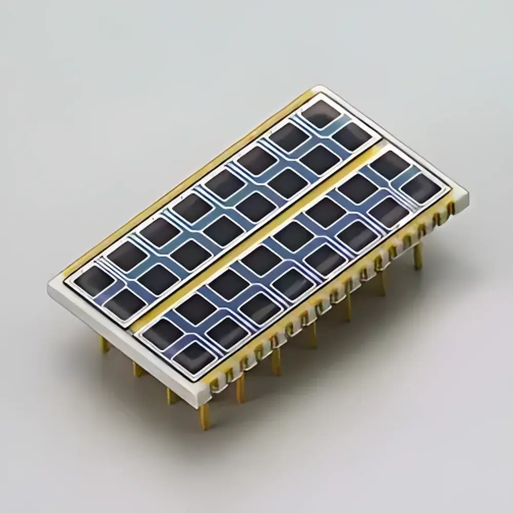
Hamamatsu S8550-02 Silicon APD Array
| Brand | Hamamatsu |
|---|---|
| Origin | Japan |
| Manufacturer Type | Original Equipment Manufacturer (OEM) |
| Import Status | Imported |
| Model | S8550-02 |
| Component Category | Optical Component |
| Type | Short-Wavelength Silicon Avalanche Photodiode Array (4 × 8 pixels) |
| Active Area per Pixel | 1.6 × 1.6 mm |
| Package | Ceramic |
| Peak Wavelength (Typ.) | 600 nm |
| Spectral Response Range (Min.) | 320–1000 nm |
| Dark Current (Max.) | 10 nA |
| Cutoff Frequency (Typ.) | 250 MHz |
| Junction Capacitance (Typ.) | 9 pF |
| Breakdown Voltage (Typ.) | 400 V |
| Temperature Coefficient of Breakdown Voltage (Typ.) | 0.78 V/°C |
| Gain (Typ.) | 50 |
| Operating Temperature | −40 to +85 °C |
| Test Condition | Ta = 25 °C, unless otherwise specified |
Overview
The Hamamatsu S8550-02 is a monolithic 4 × 8 silicon avalanche photodiode (APD) array engineered for high-sensitivity, low-noise detection in the short-wavelength spectral region (320–1000 nm). Unlike conventional PIN photodiodes, this device leverages internal gain through controlled avalanche multiplication under reverse bias near breakdown voltage—enabling photon-limited signal detection with enhanced signal-to-noise ratio (SNR) in low-light applications. Its optimized blue-response architecture delivers superior quantum efficiency at wavelengths below 500 nm, making it particularly suitable for UV–visible spectroscopy, time-resolved fluorescence detection, and laser-induced breakdown spectroscopy (LIBS) systems where spectral fidelity and temporal resolution are critical. The device operates in linear mode with stable, temperature-compensated gain—ensuring reproducible responsivity across all 32 pixels without requiring individual pixel calibration.
Key Features
- Monolithic 4 × 8 silicon APD array with uniform pixel geometry and integrated bias distribution network
- Low junction capacitance (9 pF typical) enabling high-bandwidth operation up to 250 MHz cutoff frequency
- Controlled gain of 50 (typ.) at 400 V bias, with < ±5% inter-pixel gain variation for consistent multi-channel signal scaling
- Minimal inter-pixel crosstalk (< −40 dB), achieved via deep trench isolation and optimized anode segmentation
- Ceramic hermetic package ensuring long-term stability under thermal cycling and humidity exposure
- Non-magnetic construction compatible with high-field magnetic resonance environments and ultra-high vacuum (UHV) optical setups
- Low dark current (≤10 nA at 25 °C) supporting extended integration times in photon-starved measurement regimes
Sample Compatibility & Compliance
The S8550-02 is designed for integration into OEM optical subsystems requiring spatially resolved, analog-intensity readout in the UV–NIR range. It interfaces directly with transimpedance amplifier (TIA) arrays or custom ASIC front-ends compliant with IEEE 1241-2010 ADC testing guidelines. While not a standalone instrument, its performance characteristics meet foundational requirements for ISO/IEC 17025-accredited laboratories performing optical detector characterization—including linearity verification per ISO 11146, noise-equivalent power (NEP) assessment per ANSI Z90.1, and spectral responsivity calibration traceable to NIST SRM 2020. The device conforms to RoHS Directive 2011/65/EU and REACH Regulation (EC) No. 1907/2006, with full material declaration available upon request.
Software & Data Management
As a bare-component photodetector, the S8550-02 does not include embedded firmware or native software drivers. However, Hamamatsu provides comprehensive application notes (e.g., “AN-001: Biasing and Thermal Management of Linear-Mode APDs”) and SPICE-compatible behavioral models for circuit simulation in Cadence Virtuoso and LTspice. When integrated into data acquisition systems, the array supports synchronized multi-channel sampling compliant with USB 3.0 Vision or Camera Link HS protocols when paired with appropriate frame grabbers. For GLP/GMP-regulated environments, users may implement audit-trail-capable data logging using third-party platforms such as LabVIEW NXG or MATLAB Production Server—with metadata tagging for bias voltage, temperature, and integration time to satisfy FDA 21 CFR Part 11 electronic record requirements.
Applications
- Multi-channel spectrometer detectors for compact UV–VIS absorption and reflectance analyzers
- Time-of-flight (ToF) light detection units in portable LIBS and Raman spectrometers
- Fluorescence lifetime imaging (FLIM) sensor elements in confocal and multiphoton microscopy OEM modules
- Beam profiling and wavefront sensing in adaptive optics test benches
- High-speed optical encoder feedback systems requiring sub-nanosecond timing precision
- UV-curable resin monitoring in industrial 3D printing process control loops
FAQ
What is the recommended operating bias voltage for optimal SNR?
The S8550-02 achieves maximum gain-to-noise ratio at 390–410 V reverse bias; precise setting requires temperature compensation using the stated 0.78 V/°C coefficient.
Can this APD array be cooled to reduce dark current?
Yes—operation down to −40 °C is specified; thermoelectric cooling improves dark current by ~50% per 10 °C reduction, but requires mechanical decoupling to avoid microphonic noise.
Is window transmission data available for the ceramic package?
The standard hermetic lid uses UV-grade fused silica with >90% transmission from 320–1000 nm; Hamamatsu provides spectral transmittance curves in datasheet revision D.
How is pixel-to-pixel gain uniformity verified during manufacturing?
Each wafer lot undergoes monochromatic (633 nm HeNe) photoresponse mapping at fixed bias and temperature, with pass/fail thresholds defined per JIS C 5063-2:2021.
Does Hamamatsu offer evaluation boards for this array?
Yes—the C13090-01 evaluation kit includes adjustable HV bias supply, TIA board with selectable gain (10⁴–10⁶ V/A), and SMA-triggered synchronization interface.


