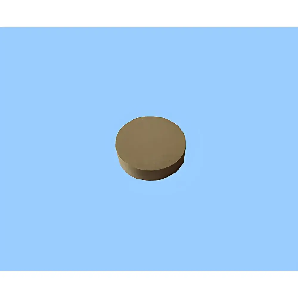
Hefei Kejing Ceramic Sputtering Targets
| Brand | Hefei Kejing |
|---|---|
| Origin | Anhui, China |
| Manufacturer Type | Authorized Distributor |
| Product Origin | Domestic (China) |
| Model | Ceramic Sputtering Targets |
| Pricing | Upon Request |
| Purity | ≥99.99% (4N) |
| Relative Density | >80% |
| Max Diameter | 76.2 mm (3 inches) |
| Material Forms | Oxides, Perovskites, Complex Ceramics |
Overview
Hefei Kejing Ceramic Sputtering Targets are high-performance thin-film deposition materials engineered for physical vapor deposition (PVD) processes—including DC/RF magnetron sputtering and pulsed laser deposition (PLD). These targets consist of stoichiometric, phase-pure ceramic compounds fabricated via controlled solid-state reaction, high-pressure cold isostatic pressing (CIP), and high-temperature sintering (>1500 °C) in precisely regulated atmospheres. Their microstructural integrity—characterized by uniform grain distribution, minimal secondary phase segregation, and low porosity—ensures stable plasma impedance, reduced arcing, and reproducible film stoichiometry across extended runs. Designed for compatibility with industrial-scale coaters and research-grade vacuum systems, these targets support the fabrication of functional oxide thin films used in optoelectronics, ferroelectric memory devices, high-temperature superconductors, transparent conductive oxides (TCOs), and solid oxide fuel cell (SOFC) electrolytes.
Key Features
- Ultra-high purity: ≥99.99% (4N) elemental composition, verified by ICP-MS and GDMS analysis
- Density optimization: >80% theoretical density achieved through optimized sintering profiles and dopant-controlled grain growth inhibition
- Phase homogeneity: Confirmed via X-ray diffraction (XRD) with Rietveld refinement; no detectable impurity phases above 0.5 wt%
- Dimensional precision: Tolerance ≤ ±0.2 mm on diameter and thickness; surface flatness <5 µm PV (peak-to-valley)
- Custom geometry support: Available in circular (up to 76.2 mm Ø), rectangular, and segmented configurations per customer specifications
- Backplate bonding readiness: All oxide-based targets are manufactured with surface finish and thermal expansion compatibility suitable for indium or epoxy bonding to copper or stainless-steel backing plates
Sample Compatibility & Compliance
These ceramic targets are compatible with standard UHV-compatible sputter chambers operating at base pressures ≤5×10⁻⁸ Torr and working gas pressures of 1–15 mTorr (Ar/O2 mixtures). They meet material traceability requirements under ISO 9001:2015-certified production workflows. Batch-specific certificates of analysis (CoA) include full XRD patterns, SEM micrographs, density measurements (Archimedes method), and impurity screening reports. For regulated environments—including semiconductor pilot lines and medical device R&D labs—the targets support GLP-aligned documentation packages and can be supplied with lot-level traceability for FDA 21 CFR Part 11-compliant data management upon request.
Software & Data Management
While the targets themselves are passive consumables, Hefei Kejing provides digital material passports accessible via secure client portal. Each batch ID links to downloadable technical datasheets, CoAs, safety data sheets (SDS), and sputtering parameter recommendations (e.g., optimal power density, target conditioning protocols, and oxygen partial pressure windows for reactive deposition). Integration with laboratory information management systems (LIMS) is supported via CSV and XML export formats for raw material inventory tracking and quality audit trails.
Applications
- Optical coatings: CeO2, TiO2, SiO2 for anti-reflective, high-reflection, and filter stacks
- Ferroelectric and piezoelectric thin films: BaTiO3, Pb(Zr,Ti)O3 (PZT), Ba0.5Sr0.5TiO3 for MEMS actuators and non-volatile memory
- High-temperature superconductors: YBCO (YBa2Cu3O7−x) for coated conductor R&D and Josephson junction fabrication
- Transparent conducting oxides: ITO, La-doped BaSnO3, and Nb-doped TiO2 for flexible electronics and photovoltaic electrodes
- Electrolyte and electrode layers: YSZ (Yttria-Stabilized Zirconia), GDC (Gd-doped CeO2), and LSCF (La0.6Sr0.4Co0.2Fe0.8O3−δ) for SOFC and sensor development
- Multiferroic and colossal magnetoresistive oxides: LSMO, LNO, BFO, and related perovskite variants for spintronics and neuromorphic device prototyping
FAQ
What is the recommended bonding method for oxide ceramic targets?
Indium solder bonding is preferred for thermal cycling stability and low interfacial resistance; epoxy bonding is acceptable for low-power applications (<5 W/cm²) where thermal management is less critical.
Can custom stoichiometries or doped variants be produced?
Yes—Hefei Kejing supports tailored compositions, including A-site/B-site doping, oxygen non-stoichiometry control, and nanostructured composite targets (e.g., metal-ceramic nanocomposites), subject to minimum order quantities and process validation timelines.
How is target erosion uniformity ensured during sputtering?
Targets are manufactured with strict control over grain size distribution (<5 µm average) and secondary phase dispersion to minimize preferential sputtering and promote azimuthally symmetric erosion profiles under balanced magnetron fields.
Are targets available with pre-polished surfaces or specific surface roughness specifications?
Standard Ra ≤ 0.8 µm is maintained; Ra ≤ 0.2 µm mirror finish and textured surfaces (e.g., for enhanced plasma confinement) are available as optional upgrades.
Do you provide sputtering yield data or film deposition rate benchmarks?
Empirical deposition rate data (nm/min/W) and stoichiometric transfer ratios (film/target composition) are provided per material system based on reference chamber conditions (e.g., AJA Orion, Lesker Lab 18) and published in application notes upon request.